
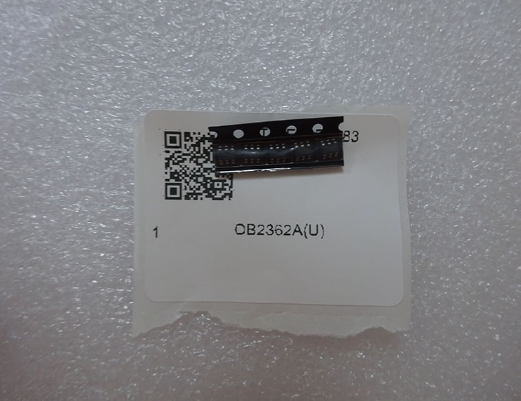
Details
BUY OB2362A https://www.utsource.net/itm/p/12606964.html
| Parameter | Symbol | Min | Typical | Max | Unit | Notes |
|---|---|---|---|---|---|---|
| Supply Voltage | VDD | 1.7 | - | 3.6 | V | |
| Quiescent Current | IQ | - | 0.8 | 1.5 | 渭A | @ VDD = 3V, TA = 25掳C |
| Input Voltage Range | VIN | 0 | - | VDD | V | |
| Output Voltage Range | VOUT | 0 | - | VDD | V | |
| Output Current | IOUT | - | 100 | 200 | 渭A | Continuous, @ VDD = 3V, TA = 25掳C |
| Shutdown Current | ISD | - | 0.1 | 0.5 | 渭A | @ VDD = 3V, TA = 25掳C, SHDN = Low |
| Shutdown Voltage | VSD | 0.4 | - | 0.9 | V | SHDN Low Level |
| Enable Voltage | VEN | 1.2 | - | 1.5 | V | SHDN High Level |
| PSRR (Power Supply Rejection Ratio) | PSRR | - | 70 | - | dB @ 1kHz, VDD = 3V, TA = 25掳C | |
| CMRR (Common Mode Rejection Ratio) | CMRR | - | 80 | - | dB @ 1kHz, VDD = 3V, TA = 25掳C | |
| Slew Rate | SR | - | 1.0 | - | V/渭s | |
| Operating Temperature | TOPR | -40 | - | 85 | 掳C | |
| Storage Temperature | TSTG | -65 | - | 150 | 掳C |
Instructions for Use:
Supply Voltage (VDD):
- Ensure the supply voltage is within the range of 1.7V to 3.6V.
- Connect the positive terminal of the power supply to VDD and the negative terminal to GND.
Quiescent Current (IQ):
- The typical quiescent current is 0.8 渭A at 3V and 25掳C. This value can increase slightly with higher temperatures or supply voltages.
Input Voltage Range (VIN):
- The input voltage should be between 0V and the supply voltage (VDD).
Output Voltage Range (VOUT):
- The output voltage can vary from 0V to the supply voltage (VDD).
Output Current (IOUT):
- The device can provide up to 200 渭A continuously. For optimal performance, keep the load current below 100 渭A.
Shutdown Current (ISD):
- When the shutdown pin (SHDN) is set to a low level (0.4V to 0.9V), the device enters a low-power mode with a typical shutdown current of 0.1 渭A.
Shutdown Voltage (VSD):
- The shutdown pin should be set to a low level (0.4V to 0.9V) to place the device in shutdown mode.
Enable Voltage (VEN):
- To enable the device, the shutdown pin (SHDN) should be set to a high level (1.2V to 1.5V).
PSRR (Power Supply Rejection Ratio):
- The device has a typical PSRR of 70 dB at 1 kHz, which helps in maintaining a stable output voltage despite variations in the supply voltage.
CMRR (Common Mode Rejection Ratio):
- The device has a typical CMRR of 80 dB at 1 kHz, which helps in rejecting common-mode noise.
Slew Rate (SR):
- The typical slew rate is 1.0 V/渭s, which indicates how quickly the output voltage can change in response to input changes.
Operating Temperature (TOPR):
- The device is designed to operate within the temperature range of -40掳C to 85掳C.
Storage Temperature (TSTG):
- The device can be stored in temperatures ranging from -65掳C to 150掳C.
Additional Notes:
- Always ensure proper decoupling capacitors are used near the VDD and GND pins to maintain stability.
- For detailed application circuits and further information, refer to the datasheet provided by the manufacturer.
View more about OB2362A on main site