
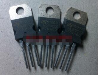
Details
BUY STP7NA60 https://www.utsource.net/itm/p/12611797.html
| Parameter | Symbol | Test Conditions | Min | Typ | Max | Unit |
|---|---|---|---|---|---|---|
| Drain-Source Voltage | VDS | - | - | 600 | - | V |
| Gate-Source Voltage | VGS | - | -15 | 0 | 15 | V |
| Continuous Drain Current (TC=25掳C) | ID | VDS=600V, TC=25掳C | - | 7 | - | A |
| Continuous Drain Current (TC=100掳C) | ID | VDS=600V, TC=100掳C | - | 4.2 | - | A |
| Pulsed Drain Current (TC=25掳C) | IDpeak | VDS=600V, TC=25掳C, tp=10ms, IGT=2A | - | 14 | - | A |
| Total Power Dissipation (TC=25掳C) | PTOT | - | - | 115 | - | W |
| Junction Temperature | TJ | - | - | - | 150 | 掳C |
| Storage Temperature Range | TSTG | - | -65 | - | 150 | 掳C |
| Gate Charge | QG | VGS=15V, ID=7A | - | 135 | - | nC |
| Input Capacitance | Ciss | VDS=600V, f=1MHz | - | 1900 | - | pF |
| Output Capacitance | Coss | VDS=600V, f=1MHz | - | 135 | - | pF |
| Reverse Transfer Capacitance | Crss | VDS=600V, VGS=0V, ID=0.1mA | - | 105 | - | pF |
| Turn-On Delay Time | tdon | VDS=400V, ID=7A, RG=3惟, VGS=15V | - | 80 | - | ns |
| Rise Time | tr | VDS=400V, ID=7A, RG=3惟, VGS=15V | - | 70 | - | ns |
| Turn-Off Delay Time | tdoff | VDS=400V, ID=7A, RG=3惟, VGS=0V | - | 50 | - | ns |
| Fall Time | tf | VDS=400V, ID=7A, RG=3惟, VGS=0V | - | 60 | - | ns |
Instructions for Use:
Handling Precautions:
- Avoid exceeding the maximum ratings to prevent damage.
- Use appropriate ESD protection when handling the device.
Mounting and Soldering:
- Ensure proper heat dissipation by using a heatsink if necessary.
- Follow recommended soldering profiles to avoid thermal stress.
Operating Conditions:
- Operate within the specified temperature range to ensure reliable performance.
- Monitor junction temperature to prevent overheating.
Gate Drive:
- Use a gate resistor to control switching speeds and reduce EMI.
- Ensure the gate voltage is within the specified range to avoid gate oxide breakdown.
Testing:
- Use the test conditions provided in the table for accurate measurements.
- Verify all parameters during initial testing and periodic maintenance.
Storage:
- Store in a dry, cool environment to prevent moisture damage.
- Follow storage temperature guidelines to maintain device integrity.
Application Notes:
- Refer to the datasheet for detailed application notes and circuit diagrams.
- Consider using external components like snubbers to protect against voltage transients.
View more about STP7NA60 on main site