
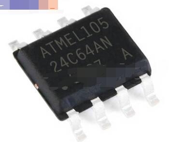
Details
BUY AT24C64AN https://www.utsource.net/itm/p/12611887.html
| Parameter | Symbol | Conditions | Min | Typical | Max | Unit |
|---|---|---|---|---|---|---|
| Operating Voltage | VCC | Continuous | 1.8 | - | 5.5 | V |
| Standby Current | ICC(S) | VCC = 5.5V, VIL | - | 1 | - | 渭A |
| Active Current | ICC(A) | VCC = 5.5V, VIH | - | 3 | - | mA |
| Write Cycle Time | tWC | VCC = 1.8V to 5.5V | - | 5 | - | ms |
| Page Write Time | tPW | VCC = 1.8V to 5.5V | - | 5 | - | ms |
| Data Retention Time | tRET | - | - | 100 | - | years |
| Number of Write Cycles | NWC | Per Byte | - | 1,000,000 | - | cycles |
| Operating Temperature Range | Toper | - | -40 | - | 85 | 掳C |
| Storage Temperature Range | Tstg | - | -65 | - | 150 | 掳C |
Instructions for Using AT24C64AN
Power Supply:
- Ensure the operating voltage (VCC) is within the range of 1.8V to 5.5V.
- Connect the ground (GND) pin to the system ground.
Addressing:
- The AT24C64AN has a 7-bit I2C address, which can be configured using the A0, A1, and A2 pins.
- The default address is 0x50 (1010000b).
Data Read/Write:
- To read data, initiate a start condition, send the device address with the read bit set, and then read the data bytes.
- To write data, initiate a start condition, send the device address with the write bit set, send the memory address, and then send the data bytes.
Write Protection:
- Use the WP (Write Protect) pin to prevent accidental writes. Set WP high to enable write protection.
Timing Considerations:
- Ensure that the write cycle time (tWC) and page write time (tPW) are respected to avoid data corruption.
- The typical write cycle time is 5 ms.
Data Retention:
- The device retains data for up to 100 years under normal operating conditions.
Temperature Range:
- Operate the device within the temperature range of -40掳C to 85掳C for optimal performance.
- Store the device within the temperature range of -65掳C to 150掳C.
Handling:
- Handle the device with care to avoid static discharge, which can damage the internal circuits.
- Use proper ESD (Electrostatic Discharge) protection when handling the device.
Programming:
- Refer to the datasheet for detailed programming sequences and timing diagrams to ensure correct operation.
Testing:
- Verify the functionality of the device by performing read and write operations and checking the data integrity.
For more detailed information, refer to the official AT24C64AN datasheet provided by the manufacturer.
(For reference only)View more about AT24C64AN on main site