
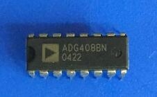
Details
BUY ADG408BN https://www.utsource.net/itm/p/12611893.html
| Parameter | Description | Min | Typ | Max | Unit |
|---|---|---|---|---|---|
| Supply Voltage (VDD) | Operating supply voltage range | 2.7 | - | 15 | V |
| Quiescent Current (IQ) | Supply current with no switches active | - | 60 | - | 渭A |
| On-Resistance (RON) | Resistance when switch is on, typical at VDD = 5V | - | 3.5 | - | 惟 |
| Leakage Current (ILK) | Maximum leakage current through switch when off | - | - | 100 | nA |
| Input Signal Range | Input signal range relative to supply rails | -0.3 | - | VDD + 0.3 | V |
| Switching Time (tON, tOFF) | Time for switch to turn on or off | - | 1 | - | 渭s |
| Storage Temperature (TSTG) | Temperature range for storage | -65 | - | 150 | 掳C |
| Operating Temperature (TOPR) | Temperature range for operation | -40 | - | 85 | 掳C |
Instructions for Use:
Power Supply:
- Ensure the supply voltage (VDD) is within the specified range of 2.7V to 15V.
- Connect the VDD pin to the positive supply and GND pin to the ground.
Signal Input:
- The input signal should be within the range of -0.3V to VDD + 0.3V to avoid damaging the device.
Switch Control:
- Use the control inputs (IN1 to IN8) to select which channel is connected to the common output (COM).
- Apply a logic high (VDD) to the control input to turn the corresponding switch on, and a logic low (GND) to turn it off.
Quiescent Current:
- The quiescent current is typically 60 渭A when no switches are active. Ensure this is accounted for in your power budget.
On-Resistance:
- The on-resistance (RON) is typically 3.5 惟 at VDD = 5V. Consider this resistance in your circuit design, especially if high precision is required.
Leakage Current:
- The maximum leakage current through a switch when it is off is 100 nA. This can be significant in low-current applications.
Temperature Considerations:
- Store the device within the temperature range of -65掳C to 150掳C.
- Operate the device within the temperature range of -40掳C to 85掳C to ensure reliable performance.
Switching Time:
- The switching time (tON, tOFF) is typically 1 渭s. This is important for applications requiring fast switching.
Handling:
- Handle the device with care to avoid electrostatic discharge (ESD) damage. Use proper ESD protection measures.
Layout:
- Ensure a clean and stable power supply by using appropriate decoupling capacitors close to the VDD and GND pins.
- Keep signal traces short to minimize noise and interference.
View more about ADG408BN on main site