
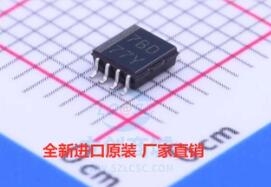
Details
BUY PCA9306DCT https://www.utsource.net/itm/p/12611993.html
| Parameter | Symbol | Min | Typ | Max | Unit | Description |
|---|---|---|---|---|---|---|
| Supply Voltage | VDD | 1.0 | - | 5.5 | V | Operating supply voltage range |
| Operating Temperature | Toper | -40 | - | 85 | 掳C | Operating temperature range |
| Input Leakage Current | IIH | - | 1 | 10 | 渭A | Maximum input leakage current at VIH |
| Output Leakage Current | IOZ | - | 1 | 10 | 渭A | Maximum output leakage current at VOH |
| Propagation Delay | tpd | 6 | - | 12 | ns | Time delay from input edge to output edge |
| Power Dissipation | PD | - | - | 100 | mW | Maximum power dissipation |
Instructions for PCA9306DCT
Power Supply Connection:
- Connect the VDD pin to the positive supply within the specified range (1.0V to 5.5V).
- Ensure a stable ground connection.
Signal Routing:
- Route input signals to the appropriate input pins.
- Ensure signal integrity by minimizing trace lengths and using proper PCB layout practices.
Temperature Management:
- Operate within the specified temperature range (-40掳C to 85掳C) to ensure reliable performance.
- Consider thermal management techniques if operating near the upper temperature limit.
Handling Static Electricity:
- The device is sensitive to ESD; handle with care and use appropriate ESD protection measures.
Timing Considerations:
- Account for propagation delays in your timing calculations, especially in high-speed applications.
Power Dissipation:
- Ensure that the total power dissipation does not exceed 100mW to avoid overheating and potential damage.
Testing and Verification:
- After assembly, verify connections and perform functional tests to ensure the device operates correctly.
View more about PCA9306DCT on main site