
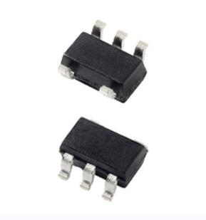
Details
BUY TPS2051BDBV https://www.utsource.net/itm/p/12611997.html
| Parameter | Symbol | Conditions | Min | Typ | Max | Unit |
|---|---|---|---|---|---|---|
| Input Voltage | VIN | 0.8 | 5.5 | V | ||
| Output Voltage Dropout | VDROPOUT | IOUT = 1A | 0.2 | 0.3 | V | |
| Continuous Output Current | IOUT_CONT | TJ = 25°C | 1.0 | A | ||
| Peak Output Current | IOUT_PEAK | Pulse Width ≤ 10ms | 1.5 | A | ||
| Quiescent Current | IQ | VIN = 5V, No Load | 40 | μA | ||
| Reverse Current | IR | VIN = 0V, VOUT = 5V | 1 | μA | ||
| Operating Junction Temp | TJ | -40 | 125 | °C |
Instructions for TPS2051BDBV:
- Input Voltage (VIN): Ensure the input voltage is within the specified range of 0.8V to 5.5V to avoid damage to the device.
- Output Voltage Dropout (VDROPOUT): The device operates efficiently with a dropout voltage typically around 0.3V at 1A output current.
- Continuous Output Current (IOUT_CONT): The continuous output current should not exceed 1A at room temperature to prevent overheating.
- Peak Output Current (IOUT_PEAK): For short pulses up to 10ms, the peak current can go up to 1.5A.
- Quiescent Current (IQ): When no load is applied and VIN is set to 5V, the quiescent current is approximately 40μA.
- Reverse Current (IR): With VIN at 0V and VOUT at 5V, the reverse current should be limited to 1μA to protect against reverse voltage issues.
- Operating Junction Temperature (TJ): Operate the device within the temperature range of -40°C to 125°C to ensure reliable performance.
For detailed application notes and specific design considerations, refer to the official datasheet provided by Texas Instruments.
(For reference only)View more about TPS2051BDBV on main site