
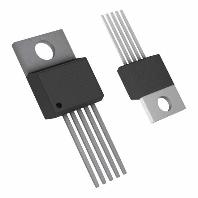
Details
BUY LT1074IT#06PBF https://www.utsource.net/itm/p/12612027.html
| Parameter | Symbol | Conditions | Min | Typ | Max | Unit |
|---|---|---|---|---|---|---|
| Input Voltage Range | VIN | - | 3.0 | - | 40.0 | V |
| Output Voltage Range | VOUT | - | 1.23 | - | 37.0 | V |
| Quiescent Current | IQ | VIN = 5V, VOUT = 5V | - | 4.5 | - | mA |
| Dropout Voltage | VDROPOUT | IOUT = 1A | - | 1.8 | - | V |
| Load Regulation | - | IOUT = 0 to 1A | - | 0.01 | - | % |
| Line Regulation | - | VIN = 5 to 40V | - | 0.01 | - | % |
| Output Current | IOUT | - | - | 1.5 | - | A |
| Power Supply Rejection | PSRR | f = 1kHz | - | 80 | - | dB |
| Operating Temperature Range | TOPR | - | -40 | - | 125 | 掳C |
| Storage Temperature Range | TSTG | - | -65 | - | 150 | 掳C |
Instructions for Using LT1074IT#06PBF
Input Voltage (VIN):
- Ensure the input voltage is within the range of 3.0V to 40.0V.
- Use appropriate input filtering capacitors to stabilize the input voltage.
Output Voltage (VOUT):
- The output voltage can be adjusted using external resistors. The formula for calculating the output voltage is: [ V_ = 1.23 left(1 + fracright) ]
- Choose R1 and R2 such that the desired output voltage is achieved.
Quiescent Current (IQ):
- The quiescent current is typically 4.5mA at VIN = 5V and VOUT = 5V. This value should be considered when designing the power supply circuit.
Dropout Voltage (VDROPOUT):
- The dropout voltage is typically 1.8V at IOUT = 1A. Ensure the input voltage is at least 1.8V higher than the desired output voltage to maintain regulation.
Load Regulation:
- The load regulation is 0.01% from 0 to 1A. This indicates minimal change in output voltage with varying load currents.
Line Regulation:
- The line regulation is 0.01% from 5V to 40V. This indicates minimal change in output voltage with varying input voltages.
Output Current (IOUT):
- The maximum continuous output current is 1.5A. Ensure the load does not exceed this limit to avoid damage to the device.
Power Supply Rejection Ratio (PSRR):
- The PSRR is 80dB at 1kHz. This indicates good rejection of ripple and noise from the input supply.
Operating Temperature Range (TOPR):
- The device operates reliably from -40掳C to 125掳C. Ensure the ambient temperature is within this range.
Storage Temperature Range (TSTG):
- The device can be stored from -65掳C to 150掳C without damage.
PCB Layout:
- Use a ground plane to reduce noise and improve thermal performance.
- Place input and output capacitors close to the device to minimize parasitic inductance.
Thermal Considerations:
- If operating at high output currents or in high ambient temperatures, ensure adequate heat sinking to keep the junction temperature below the maximum rating.
Protection Features:
- The device includes thermal shutdown and current limiting to protect against overtemperature and overload conditions.
By following these guidelines, you can ensure reliable operation of the LT1074IT#06PBF in your application.
(For reference only)View more about LT1074IT#06PBF on main site