
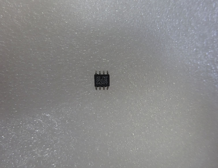
Details
BUY OP213ESZ https://www.utsource.net/itm/p/12612039.html
| Parameter | Symbol | Conditions | Min | Typical | Max | Unit |
|---|---|---|---|---|---|---|
| Supply Voltage | VCC | Operating Range | 2.7 | - | 5.5 | V |
| Input Offset Voltage | VIO | VCC = 5V, TA = 25°C | -100 | 25 | 100 | μV |
| Input Bias Current | IB | VCC = 5V, TA = 25°C | -5 | 0.5 | 5 | nA |
| Input Voltage Noise Density | en | VCC = 5V, TA = 25°C, f = 1kHz | - | 2.7 | - | nV/√Hz |
| Output Voltage Swing | VOS | VCC = 5V, TA = 25°C, RL = 10kΩ | 0.01 | - | 5.49 | V |
| Slew Rate | SR | VCC = 5V, TA = 25°C | - | 0.3 | - | V/μs |
| Bandwidth | f-3dB | VCC = 5V, TA = 25°C, G = +1 | - | 1.2 | - | MHz |
| Common-Mode Rejection Ratio | CMRR | VCC = 5V, TA = 25°C, f = 60Hz | 86 | - | 120 | dB |
| Power Supply Rejection Ratio | PSRR | VCC = 5V, TA = 25°C, f = 60Hz | 86 | - | 120 | dB |
| Quiescent Current | IQ | VCC = 5V, TA = 25°C | - | 100 | - | μA |
Instructions for Use:
- Supply Voltage: Ensure the supply voltage is within the operating range of 2.7V to 5.5V.
- Input Signals: Keep input signals within the common-mode input voltage range, which is typically from 0V to VCC - 1.5V.
- Output Load: Connect a load resistor (RL) of at least 10kΩ to ensure proper output voltage swing.
- Temperature Considerations: The device is designed to operate at temperatures ranging from -40°C to 125°C, but performance parameters are typically specified at 25°C.
- Power Supply Decoupling: Use decoupling capacitors (e.g., 0.1μF and 10μF) close to the power supply pins to minimize noise and ensure stable operation.
- Slew Rate Limitation: Be aware of the slew rate limitation when designing circuits that require fast signal transitions.
- Noise Considerations: For low-noise applications, consider the input voltage noise density and use appropriate filtering if necessary.
- Stability: Ensure the feedback network is designed to maintain stability, especially in high-gain configurations.
For more detailed information, refer to the datasheet provided by the manufacturer.
(For reference only)View more about OP213ESZ on main site