
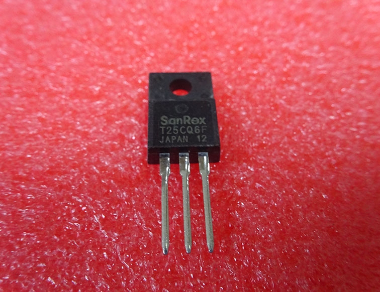
Details
BUY T25CQ6F https://www.utsource.net/itm/p/12612049.html
| Parameter | Symbol | Min | Typ | Max | Unit | Description |
|---|---|---|---|---|---|---|
| Supply Voltage | VDD | 1.7 | - | 3.6 | V | Operating voltage range |
| Output Current | IO | - | 20 | - | mA | Maximum output current per I/O pin |
| Standby Current | ISB | - | 1 | - | 渭A | Typical standby current at VDD = 3.0V, TA = 25掳C |
| Operating Temperature | TOPR | -40 | - | 85 | 掳C | Operating temperature range |
| Storage Temperature | TSTG | -65 | - | 150 | 掳C | Storage temperature range |
| Input Capacitance | CIN | - | 10 | - | pF | Input capacitance at VDD = 3.0V, f = 1 MHz |
| Output Leakage Current | IOL | - | 1 | - | 渭A | Output leakage current at VDD = 3.0V |
| Rise Time | tr | - | 10 | - | ns | Rise time from 10% to 90% of VDD |
| Fall Time | tf | - | 10 | - | ns | Fall time from 90% to 10% of VDD |
Instructions for Using T25CQ6F
Power Supply:
- Ensure the supply voltage (VDD) is within the specified range of 1.7V to 3.6V.
- Use a stable power source to avoid fluctuations that could affect performance.
Pin Configuration:
- Refer to the datasheet for the correct pin configuration to ensure proper connection.
- Connect the VDD pin to the positive supply and GND to the ground.
Output Handling:
- Do not exceed the maximum output current (IO) of 20mA per I/O pin to prevent damage.
- Use appropriate external components (e.g., resistors) to limit current if necessary.
Temperature Considerations:
- Operate the device within the specified operating temperature range (-40掳C to 85掳C).
- Store the device within the storage temperature range (-65掳C to 150掳C) to avoid degradation.
Signal Integrity:
- Keep signal lines as short as possible to minimize noise and interference.
- Use decoupling capacitors close to the VDD and GND pins to filter out high-frequency noise.
Standby Mode:
- To reduce power consumption, use the standby mode where the typical current is 1渭A.
- Ensure that the device is properly configured to enter and exit standby mode without data loss.
Capacitance and Leakage:
- Be aware of the input capacitance (10pF) when designing circuits with high-frequency signals.
- Account for the output leakage current (1渭A) in sensitive applications.
Timing Parameters:
- Consider the rise and fall times (10ns) when designing timing-critical applications.
- Use these parameters to ensure that the device meets the required signal transition times.
By following these guidelines, you can ensure optimal performance and reliability of the T25CQ6F in your application.
(For reference only)View more about T25CQ6F on main site