
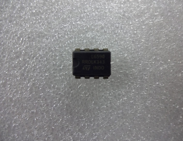
Details
BUY L6590N https://www.utsource.net/itm/p/12612050.html
| Parameter | Symbol | Min | Typical | Max | Unit |
|---|---|---|---|---|---|
| Supply Voltage | Vcc | 14 | - | 30 | V |
| Maximum Output Current | Iout | - | 1.5 | 2 | A |
| Maximum Duty Cycle | Dmax | - | 97% | - | % |
| Switching Frequency | fsw | - | 100 | 500 | kHz |
| Quiescent Current | IQ | - | 2.5 | 3 | mA |
| Shutdown Current | ISD | - | 10 | 15 | 渭A |
| Overcurrent Protection | OCP | - | 2.2 | 2.8 | A |
| Thermal Shutdown | TSD | 160 | - | - | 掳C |
| Operating Temperature | Topr | -40 | - | 125 | 掳C |
| Storage Temperature | Tstg | -40 | - | 150 | 掳C |
Instructions for Using the L6590N
Supply Voltage (Vcc):
- Ensure the supply voltage is within the range of 14V to 30V. Exceeding these limits can damage the device.
Output Current (Iout):
- The maximum continuous output current is 2A. Do not exceed this limit to avoid overheating or damage.
Switching Frequency (fsw):
- Set the switching frequency between 100kHz and 500kHz using an external resistor. The typical value is 100kHz.
Thermal Management:
- The device has a thermal shutdown feature that activates at 160掳C. Ensure proper heat sinking to prevent excessive temperature rise.
Overcurrent Protection (OCP):
- The overcurrent protection threshold is set between 2.2A and 2.8A. If the output current exceeds this range, the device will shut down to protect itself.
Quiescent and Shutdown Current:
- The quiescent current is typically 2.5mA, and the shutdown current is around 10渭A. Use the shutdown pin to reduce power consumption when the device is not in use.
Operating and Storage Temperature:
- The operating temperature range is -40掳C to 125掳C, and the storage temperature range is -40掳C to 150掳C. Ensure the device is used within these limits to maintain reliability.
Pin Configuration:
- Refer to the datasheet for the correct pin configuration and connections. Proper pin connections are crucial for the device to function correctly.
External Components:
- Use appropriate external components such as resistors, capacitors, and inductors as specified in the datasheet to ensure stable operation.
Layout Considerations:
- Follow good PCB layout practices to minimize noise and interference. Keep high-current paths short and wide, and use ground planes to reduce parasitic inductance.
View more about L6590N on main site