
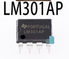
Details
BUY LM301AP https://www.utsource.net/itm/p/12612067.html
| Parameter | Symbol | Conditions | Min | Typ | Max | Unit |
|---|---|---|---|---|---|---|
| Supply Voltage | Vcc | Operating | 4.5 | - | 40 | V |
| Input Offset Voltage | Vos | Initial (Note 1) | -2 | 0 | 2 | mV |
| Input Bias Current | Ib | Differential | 20 | 80 | 300 | nA |
| Input Offset Current | Ios | (Note 2) | -10 | 0 | 10 | nA |
| Slew Rate | SR | Small Signal | - | 0.3 | - | V/μs |
| Bandwidth | f-3dB | Unity Gain | - | 1.1 | - | MHz |
| Output Voltage Swing | Vout | No Load | 0 | - | Vcc-1.5 | V |
Instructions for LM301AP:
Power Supply Connection:
- Connect the supply voltage between the V+ and V- pins. Ensure the supply voltage is within the specified range of 4.5V to 40V.
Input Configuration:
- The differential input voltage should not exceed the supply voltage range. For optimal performance, keep the common-mode input voltage within the specified limits.
Output Configuration:
- The output can swing from 0V to approximately 1.5V below the positive supply voltage. Avoid loading the output with a load that would prevent this swing range.
Biasing and Compensation:
- Proper biasing of the inputs is necessary for accurate operation. External compensation may be required depending on the application to stabilize the op-amp and achieve desired frequency response.
Handling Precautions:
- Handle the device carefully to avoid damage from electrostatic discharge (ESD). Use appropriate ESD protection measures during handling and assembly.
Mounting:
- Ensure proper mounting and soldering techniques are used to maintain thermal and electrical performance. Follow the manufacturer’s guidelines for recommended PCB layout.
(Note 1: Initial input offset voltage is measured at room temperature.) (Note 2: Input offset current is the difference between the currents into the two input terminals.)
(For reference only)View more about LM301AP on main site