
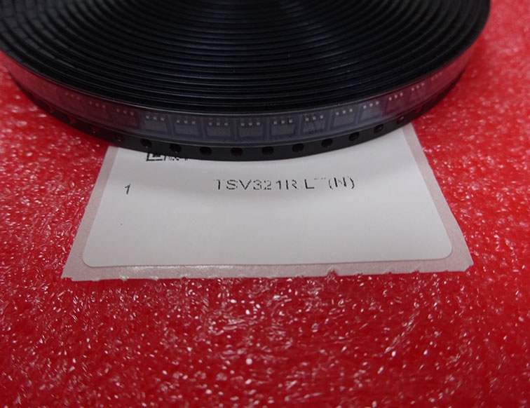
Details
BUY TSV321RILT https://www.utsource.net/itm/p/12612081.html
| Parameter | Symbol | Conditions | Min | Typ | Max | Unit |
|---|---|---|---|---|---|---|
| Supply Voltage | VCC | Operating | 2.7 | - | 5.5 | V |
| Input Offset Voltage | VIO | VCC=3V, TA=25掳C | -0.4 | 0.1 | 0.4 | mV |
| Input Bias Current | IB | VCC=3V, TA=25掳C | - | 2 | - | nA |
| Slew Rate | SR | VCC=3V, TL=1k惟, CL=10pF | - | 0.8 | - | V/渭s |
| Bandwidth | BW | VCC=3V, G=+1, RL=1k惟 | - | 1.6 | - | MHz |
| Unity Gain Bandwidth | fT | VCC=3V, TA=25掳C | - | 2.2 | - | MHz |
| Output Voltage Swing | VOS | VCC=3V, TA=25掳C, RL=1k惟 | -1.2 | - | 1.2 | V |
Instructions for Using TSV321RILT
Supply Voltage: Ensure the supply voltage (VCC) is within the range of 2.7V to 5.5V for proper operation.
Input Configuration: Be mindful of the input bias current and offset voltage when designing circuits to minimize errors in signal processing.
Output Considerations: The output voltage swing can go as low as -1.2V and as high as +1.2V relative to the supply rails. Design your load circuitry accordingly to ensure it operates within these limits.
Frequency Response: The typical unity gain bandwidth is 2.2 MHz. For applications requiring higher frequency response, verify that this meets the system requirements.
Slew Rate: With a typical slew rate of 0.8 V/渭s, consider this parameter if fast transient responses are necessary in your application.
Operating Temperature: Ensure the device operates within the specified temperature range to avoid performance degradation or damage.
Power-On Sequence: If used in conjunction with other components, ensure the power-on sequence does not exceed the operational limits of the TSV321RILT.
Decoupling Capacitors: Use appropriate decoupling capacitors close to the power pins to reduce noise and improve stability.
Handling Precautions: Handle the component carefully to avoid ESD damage. Follow standard ESD handling procedures during assembly and testing.
View more about TSV321RILT on main site