
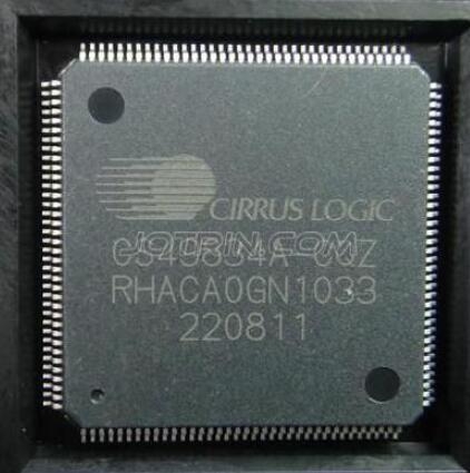
Details
BUY CS49834A-CQZ https://www.utsource.net/itm/p/12612100.html
| Parameter | Description | Value | Unit |
|---|---|---|---|
| Device Type | High Efficiency, Synchronous Step-Down DC/DC Converter | - | - |
| Input Voltage Range | Minimum Input Voltage | 2.7 | V |
| Maximum Input Voltage | 5.5 | V | |
| Output Voltage Range | Adjustable Output Voltage | 0.6 to VIN | V |
| Switching Frequency | Fixed Switching Frequency | 1.0 | MHz |
| Output Current | Continuous Output Current | 3.0 | A |
| Quiescent Current | Operating Quiescent Current | 20 | 渭A |
| Shutdown Current | Shutdown Mode Current | 0.1 | 渭A |
| Efficiency | Typical Efficiency at 3.3V In, 1.8V Out, 1A Load | 95 | % |
| Operating Temperature Range | Minimum Operating Temperature | -40 | 掳C |
| Maximum Operating Temperature | 125 | 掳C | |
| Package Type | Package | QFN-16 | - |
| Pin Pitch | Pin Pitch | 0.5 | mm |
| Package Size | Package Size | 3x3 | mm |
Instructions for Use:
Input Capacitor Selection:
- Place a low ESR ceramic capacitor (10 渭F or higher) as close as possible to the input pins.
- Additional bulk capacitance may be required for stability and noise reduction.
Output Capacitor Selection:
- Use a low ESR ceramic capacitor (10 渭F or higher) for output filtering.
- Ensure the capacitor has a ripple current rating suitable for the expected load.
Inductor Selection:
- Choose an inductor with a saturation current rating higher than the maximum output current.
- Typical inductance values range from 1.0 渭H to 4.7 渭H, depending on the application requirements.
Feedback Resistor Network:
- Set the output voltage using the feedback resistor network. The formula for calculating the resistors is: [ V_ = V_ left(1 + fracright) ] where ( V_ = 0.6V ).
PCB Layout:
- Keep the power loop area small to minimize parasitic inductance.
- Place the ground plane under the device to improve thermal performance and reduce noise.
Thermal Considerations:
- Ensure adequate heat dissipation by providing a thermal pad and using a heatsink if necessary.
- Check the junction temperature during operation to ensure it remains within the operating temperature range.
Shutdown Function:
- Apply a logic high signal to the SHDN pin to enable the device.
- Apply a logic low signal to the SHDN pin to disable the device and enter shutdown mode.
Stability:
- Use the recommended external components to ensure the converter operates stably over the entire input voltage and load range.
Safety:
- Ensure all connections are secure and insulated to prevent short circuits.
- Follow proper handling procedures to avoid damage to the device.
View more about CS49834A-CQZ on main site