
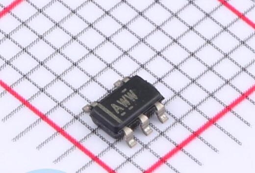
Details
BUY TPS79925DDCTG4 https://www.utsource.net/itm/p/12612102.html
| Parameter | Symbol | Min | Typical | Max | Unit | Conditions |
|---|---|---|---|---|---|---|
| Input Voltage | VIN | 1.7 | 5.5 | V | ||
| Output Voltage | VOUT | 2.5 | V | Fixed output | ||
| Output Current | IOUT | 200 | mA | Continuous | ||
| Dropout Voltage | VDROPOUT | 0.28 | V | IOUT = 100 mA, VIN = 3.0 V | ||
| Quiescent Current | IQ | 1.8 | 渭A | No load, VIN = 3.3 V | ||
| Shutdown Current | ISD | 0.1 | 渭A | VIN = 3.3 V, EN = 0 V | ||
| Load Regulation | 0.2 | % | IOUT = 0 to 200 mA | |||
| Line Regulation | 0.01 | %/V | VIN = 1.7 to 5.5 V | |||
| PSRR (1 kHz) | 60 | dB | VIN = 3.3 V, IOUT = 100 mA | |||
| Operating Temperature | TJ | -40 | 125 | 掳C | ||
| Storage Temperature | TSTG | -65 | 150 | 掳C |
Instructions for Using TPS79925DDCTG4:
Input Voltage:
- Ensure the input voltage is within the range of 1.7 V to 5.5 V.
- Use appropriate decoupling capacitors on the input side to filter out noise and stabilize the input voltage.
Output Voltage:
- The TPS79925DDCTG4 provides a fixed output voltage of 2.5 V.
- Use a bypass capacitor on the output to maintain stability and reduce ripple.
Output Current:
- The device can supply up to 200 mA continuously.
- For higher current requirements, consider using a heatsink or a more powerful regulator.
Dropout Voltage:
- The dropout voltage is typically 0.28 V at 100 mA.
- Ensure that the input voltage is at least 0.28 V above the output voltage to maintain regulation.
Quiescent Current:
- The quiescent current is very low, typically 1.8 渭A, which makes the device suitable for battery-powered applications.
Shutdown Current:
- When the enable pin (EN) is set to 0 V, the shutdown current is typically 0.1 渭A, significantly reducing power consumption.
Load and Line Regulation:
- The load regulation is 0.2%, ensuring stable output voltage over a wide range of load currents.
- The line regulation is 0.01% per volt, maintaining output stability with varying input voltages.
Power Supply Rejection Ratio (PSRR):
- The PSRR at 1 kHz is 60 dB, effectively rejecting input voltage variations and noise.
Operating and Storage Temperature:
- The operating temperature range is from -40掳C to 125掳C.
- The storage temperature range is from -65掳C to 150掳C.
PCB Layout Considerations:
- Place the input and output capacitors as close as possible to the regulator to minimize trace inductance and improve transient response.
- Use wide and short traces for power paths to reduce resistance and inductance.
Enable Pin:
- The enable pin (EN) can be used to control the operation of the regulator. Connect it to VCC to enable the regulator and to GND to disable it.
Thermal Management:
- If operating at high temperatures or under high current conditions, ensure adequate heat dissipation by using a heatsink or a thermal pad.
By following these guidelines, you can ensure optimal performance and reliability of the TPS79925DDCTG4 in your application.
(For reference only)View more about TPS79925DDCTG4 on main site