
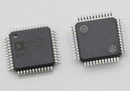
Details
BUY ADV7125KSTZ140 https://www.utsource.net/itm/p/12612121.html
| Parameter | Description | Min | Typ | Max | Unit |
|---|---|---|---|---|---|
| Supply Voltage (VDD) | Operating supply voltage | 3.0 | - | 3.6 | V |
| Differential Input Voltage | Maximum differential input voltage | -0.3 | - | 0.3 | V |
| Output Voltage Swing | Output voltage swing (into 150惟 load) | 0.2 | - | 0.8 | Vpp |
| Output Current | Maximum output current | - | - | 30 | mA |
| Bandwidth | Analog bandwidth | - | 350 | - | MHz |
| Power Consumption | Typical power consumption | - | 270 | - | mW |
| Rise Time | Rise time (10% to 90%) | - | 1.4 | - | ns |
| Fall Time | Fall time (90% to 10%) | - | 1.4 | - | ns |
| Slew Rate | Slew rate | - | 1000 | - | V/渭s |
| Differential Gain | Differential gain error | -0.5 | 0 | 0.5 | % |
| Differential Phase | Differential phase error | -0.5 | 0 | 0.5 | 掳 |
| Harmonic Distortion | Second harmonic distortion at 10 MHz | -60 | - | - | dBc |
| Third Harmonic Distortion | Third harmonic distortion at 10 MHz | -60 | - | - | dBc |
| SNR | Signal-to-noise ratio | - | 65 | - | dB |
| Operating Temperature | Operating temperature range | -40 | - | 85 | 掳C |
| Storage Temperature | Storage temperature range | -65 | - | 150 | 掳C |
Instructions for Use:
Power Supply:
- Ensure the supply voltage (VDD) is within the range of 3.0V to 3.6V.
- Use a stable and clean power source to avoid noise and instability.
Input Signals:
- The differential input voltage should not exceed 卤0.3V to prevent damage to the device.
- Connect the input signals to the appropriate pins as specified in the datasheet.
Output Configuration:
- The output voltage swing is designed for a 150惟 load. Ensure the load impedance matches this value for optimal performance.
- The maximum output current is 30mA. Do not exceed this limit to avoid damaging the device.
Bandwidth and Timing:
- The analog bandwidth of 350MHz ensures high-frequency signal integrity.
- The rise and fall times of 1.4ns ensure fast signal transitions, which are crucial for high-speed applications.
Signal Quality:
- Monitor the differential gain and phase errors to ensure they remain within 卤0.5% and 卤0.5掳, respectively.
- Check the harmonic distortion and SNR to maintain signal purity and clarity.
Environmental Conditions:
- Operate the device within the temperature range of -40掳C to 85掳C for reliable performance.
- Store the device in a temperature range of -65掳C to 150掳C to prevent damage during storage.
Power-Up Sequence:
- Follow the recommended power-up sequence to ensure proper initialization and operation of the device.
Grounding and Shielding:
- Proper grounding and shielding are essential to minimize noise and interference, especially in high-frequency applications.
Testing and Validation:
- Perform initial testing and validation to ensure the device meets the required specifications and performance criteria.
Safety Precautions:
- Handle the device with care to avoid static discharge and physical damage.
- Follow all safety guidelines and regulations when working with electronic components.
View more about ADV7125KSTZ140 on main site