
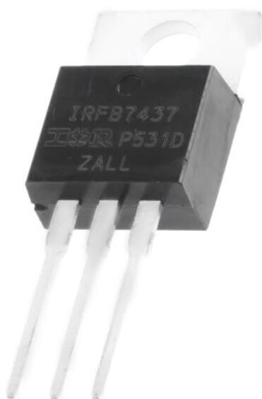
Details
BUY IRFB7437PBF https://www.utsource.net/itm/p/12612154.html
| Parameter | Symbol | Min | Typ | Max | Unit | Conditions |
|---|---|---|---|---|---|---|
| Drain-Source Voltage | VDS | -55 | - | 55 | V | |
| Gate-Source Voltage | VGS | -20 | - | 20 | V | |
| Continuous Drain Current | ID | - | 68 | - | A | TC = 25掳C |
| Pulse Drain Current | IDpeak | - | 190 | - | A | tp = 10 渭s, TC = 25掳C |
| Power Dissipation | PTOT | - | - | 210 | W | TC = 25掳C |
| Junction Temperature | TJ | - | - | 150 | 掳C | |
| Storage Temperature | TSTG | -55 | - | 150 | 掳C | |
| Thermal Resistance | R胃JC | - | 0.6 | - | 掳C/W | Junction to Case |
Instructions for Use:
Handling Precautions:
- The IRFB7437PBF is sensitive to electrostatic discharge (ESD). Handle with care and use appropriate ESD protection.
- Avoid exceeding the maximum ratings listed in the table to prevent damage.
Mounting:
- Ensure proper heat sinking to manage power dissipation and maintain the junction temperature within safe limits.
- Follow the recommended PCB layout guidelines to optimize thermal performance and minimize parasitic inductance.
Gate Drive:
- Apply a gate voltage between VGS(th) and the maximum VGS to ensure reliable operation.
- Use a gate resistor to control the switching speed and reduce electromagnetic interference (EMI).
Storage:
- Store in a dry, cool environment to prevent moisture damage.
- Follow the storage temperature range to avoid degradation.
Testing:
- Perform initial testing at room temperature to verify functionality.
- Conduct thermal cycling tests to ensure reliability under varying temperature conditions.
Application Notes:
- Refer to the datasheet for detailed application notes and circuit diagrams.
- For high-frequency applications, consider the impact of parasitic elements and layout on performance.
View more about IRFB7437PBF on main site