
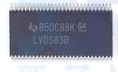
Details
BUY Texas Instruments SN75LVDS83BDGGR https://www.utsource.net/itm/p/12612155.html
| Parameter | Min | Typ | Max | Unit | Description |
|---|---|---|---|---|---|
| Supply Voltage (VCCA) | 2.7 | - | 3.6 | V | Operating supply voltage |
| Differential Input Voltage (VID) | -0.4 | - | 4.0 | V | Maximum differential input voltage |
| Common-Mode Input Voltage (VICR) | 0.5 | - | 2.7 | V | Common-mode input voltage range |
| Output Current (IOL, IOH) | - | 16 | - | mA | Output current at low and high levels |
| Propagation Delay (tPD) | - | 3.8 | - | ns | Time delay from input to output |
| Skew (tSKEW) | - | 0.4 | - | ns | Maximum difference in propagation delay between channels |
| Power Dissipation (PD) | - | - | 270 | mW | Maximum power dissipation |
| Operating Temperature Range | -40 | - | 85 | 掳C | Temperature range for operation |
| Storage Temperature Range | -65 | - | 150 | 掳C | Temperature range for storage |
Instructions for Use:
Power Supply:
- Ensure the supply voltage (VCCA) is within the specified range of 2.7V to 3.6V.
Input Signals:
- Keep the differential input voltage (VID) within -0.4V to 4.0V relative to ground.
- Maintain the common-mode input voltage (VICR) between 0.5V and 2.7V.
Output Handling:
- The device can source or sink up to 16mA per output pin.
- Be aware of the propagation delay (tPD) which is typically around 3.8ns.
Timing Considerations:
- Account for a maximum skew (tSKEW) of 0.4ns between channels when designing timing-sensitive applications.
Thermal Management:
- Ensure that the device does not exceed its maximum power dissipation of 270mW under continuous operation.
- Operate the device within the temperature range of -40掳C to 85掳C for reliable performance.
Storage Conditions:
- Store the device in an environment where temperatures do not drop below -65掳C or rise above 150掳C.
Handling Precautions:
- Handle with care to avoid electrostatic discharge (ESD) damage. Follow standard ESD handling procedures.
View more about Texas Instruments SN75LVDS83BDGGR on main site