
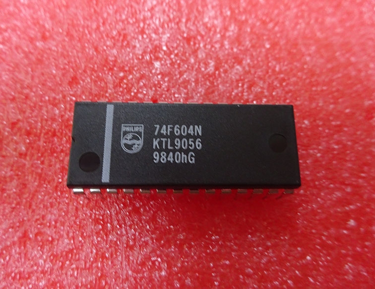
Details
BUY 74F604N https://www.utsource.net/itm/p/12612171.html
| Parameter | Symbol | Conditions | Min | Typical | Max | Unit |
|---|---|---|---|---|---|---|
| Supply Voltage | Vcc | Operating | 4.5 | - | 5.5 | V |
| Input Low Voltage | VI(L) | IIL = 1 mA | 0 | - | 0.8 | V |
| Input High Voltage | VI(H) | IIH = -20 渭A | 2.0 | - | Vcc | V |
| Output Low Voltage | VO(L) | IO = 4 mA | 0 | - | 0.4 | V |
| Output High Voltage | VO(H) | IO = -4 mA | 2.4 | - | Vcc | V |
| Propagation Delay Time | tpd | Vcc = 5V, Tamb = 25掳C | - | 3.5 | 7 | ns |
| Power Dissipation | PD | Per Package | - | - | 100 | mW |
| Operating Temperature | Tamb | -40 | - | 85 | 掳C | |
| Storage Temperature | Tstg | -65 | - | 150 | 掳C |
Instructions for Use:
Supply Voltage (Vcc):
- Ensure the supply voltage is within the specified range of 4.5V to 5.5V to avoid damage to the device.
Input Voltage Levels:
- Input voltages should be within the specified ranges to ensure proper logic levels:
- Low input voltage (VI(L)): 0V to 0.8V.
- High input voltage (VI(H)): 2.0V to Vcc.
- Input voltages should be within the specified ranges to ensure proper logic levels:
Output Voltage Levels:
- Output voltages will be:
- Low output voltage (VO(L)): 0V to 0.4V when sourcing 4 mA.
- High output voltage (VO(H)): 2.4V to Vcc when sinking 4 mA.
- Output voltages will be:
Propagation Delay Time (tpd):
- The typical propagation delay time is 3.5 ns with a maximum of 7 ns at Vcc = 5V and ambient temperature (Tamb) = 25掳C.
Power Dissipation:
- The maximum power dissipation per package is 100 mW. Ensure adequate heat dissipation if operating near this limit.
Operating Temperature (Tamb):
- The device is designed to operate within the temperature range of -40掳C to 85掳C. Avoid operating outside this range to prevent damage or reduced performance.
Storage Temperature (Tstg):
- Store the device in an environment where the temperature does not exceed -65掳C to 150掳C to maintain its integrity.
Handling Precautions:
- Handle the device with care to avoid static discharge, which can damage the sensitive components.
- Use appropriate anti-static measures when handling and storing the device.
Mounting and Soldering:
- Follow standard soldering procedures to avoid thermal shock and mechanical stress during assembly.
- Ensure that the device is properly mounted and connected to the circuit board to prevent issues such as poor electrical contact.
Testing:
- Before integrating the device into a larger system, perform initial tests to verify its functionality and performance according to the specified parameters.
View more about 74F604N on main site