
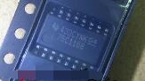
Details
BUY SN75C1168D https://www.utsource.net/itm/p/12612176.html
| Parameter | Symbol | Conditions | Min | Typ | Max | Unit |
|---|---|---|---|---|---|---|
| Supply Voltage | VCC | 4.5 | 5.5 | V | ||
| Output Voltage High | VOH | IL = -10mA | 3.9 | V | ||
| Output Voltage Low | VOL | IL = 10mA | 0.1 | V | ||
| Input Voltage High | VIH | 2.0 | V | |||
| Input Voltage Low | VIL | 0.8 | V | |||
| Propagation Delay Time | tpd | VCC = 5V, TA = 25掳C | 7 | ns | ||
| Power Dissipation | PD | 670 | mW | |||
| Operating Temperature | TOPR | -40 | 85 | 掳C |
Instructions for SN75C1168D
Power Supply:
- Ensure the supply voltage (VCC) is within the range of 4.5V to 5.5V.
Input Signals:
- For proper recognition, input voltages should be above 2.0V for logic high and below 0.8V for logic low.
Output Signals:
- The output voltage levels are designed to provide a high level of at least 3.9V when sourcing up to -10mA and a low level of no more than 0.1V when sinking up to 10mA.
Propagation Delay:
- Expect a typical propagation delay time of 7ns under standard conditions (VCC = 5V, ambient temperature = 25掳C).
Thermal Considerations:
- Operate the device within the temperature range of -40掳C to 85掳C to ensure reliable performance.
- Be mindful of power dissipation; do not exceed 670mW to avoid overheating.
Handling:
- Follow ESD precautions as the device is sensitive to electrostatic discharge.
Mounting:
- Ensure correct orientation during PCB assembly to prevent damage or malfunction.
View more about SN75C1168D on main site