
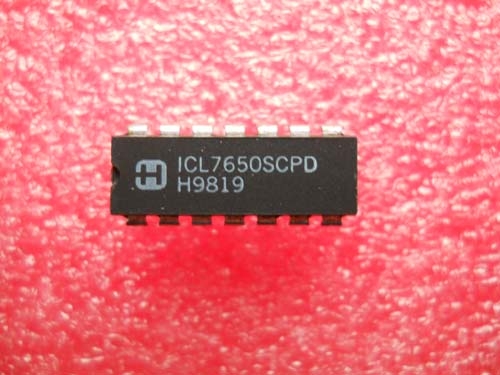
Details
BUY ICL7650SCPD https://www.utsource.net/itm/p/12612183.html
| Parameter | Symbol | Min | Typ | Max | Unit |
|---|---|---|---|---|---|
| Supply Voltage | VCC | -18 | -12 | -4.5 | V |
| Quiescent Current | IQ | - | 25 | - | 渭A |
| Input Bias Current | IB | - | 1 | - | pA |
| Input Offset Current | IOS | - | 0.1 | - | pA |
| Input Offset Voltage | VOS | - | 50 | - | 渭V |
| Common-Mode Input Voltage Range | VCM | VCC + 1.5 | - | VCC - 1.5 | V |
| Output Voltage Swing | VOUT | VCC + 1.5 | - | VCC - 1.5 | V |
| Slew Rate | SR | - | 0.3 | - | V/渭s |
| Bandwidth (Unity Gain) | fU | - | 1.5 | - | Hz |
| Gain-Bandwidth Product | GBW | - | 1.5 | - | MHz |
Instructions for Using ICL7650SCPD
Power Supply:
- Ensure the supply voltage is within the specified range (-4.5V to -18V).
- Use a stable power supply to avoid noise and instability.
Input Signals:
- The input signals should be within the common-mode input voltage range (VCC + 1.5V to VCC - 1.5V).
- Use high-impedance sources to minimize loading effects on the input.
Output Configuration:
- The output voltage swing is limited to VCC + 1.5V to VCC - 1.5V.
- Ensure that the load impedance is appropriate for the output current capabilities of the op-amp.
Biasing and Offset:
- The input bias current is very low (1 pA typical), but it can still affect high-impedance circuits.
- The input offset voltage and current should be considered in precision applications to minimize errors.
Stability and Compensation:
- The ICL7650SCPD is internally compensated for unity gain stability.
- For higher gain applications, additional external compensation may be necessary to ensure stability.
Temperature Considerations:
- The device is designed to operate over a wide temperature range, but performance parameters may vary with temperature.
- Refer to the datasheet for detailed temperature coefficients and derating curves.
Handling and Storage:
- Handle the device with care to avoid static damage.
- Store in a dry environment to prevent moisture-related issues.
PCB Layout:
- Use proper PCB layout techniques to minimize noise and parasitic effects.
- Place bypass capacitors close to the power pins to ensure stable operation.
Testing and Debugging:
- Test the circuit under various operating conditions to ensure reliable performance.
- Use a multimeter or oscilloscope to monitor key parameters such as supply voltage, input signals, and output voltage.
Safety Precautions:
- Ensure that all connections are secure and properly insulated.
- Follow standard safety guidelines when working with electronic components and circuits.
View more about ICL7650SCPD on main site