
Details
BUY AD706J https://www.utsource.net/itm/p/12612234.html
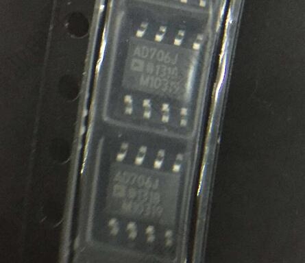
Below is the parameter table and instructions for the AD706J, a dual low power, high precision FET-input operational amplifier from Analog Devices.
AD706J Parameter Table
| Parameter | Symbol | Min | Typ | Max | Unit | Conditions |
|---|---|---|---|---|---|---|
| Supply Voltage | VCC | 2.7 | - | 36 | V | Single Supply |
| Supply Current | ICC | - | 950 | - | 渭A | Each Amplifier, VCC = 15V |
| Input Offset Voltage | VOS | - | 25 | - | 渭V | 25掳C |
| Input Bias Current | IB | - | 40 | - | pA | 25掳C |
| Input Offset Current | IIO | - | 2 | - | pA | 25掳C |
| Common-Mode Rejection Ratio (CMRR) | CMRR | - | 110 | - | dB | 25掳C, f = 0 Hz |
| Power-Supply Rejection Ratio (PSRR) | PSRR | - | 110 | - | dB | 25掳C, f = 0 Hz |
| Slew Rate | SR | - | 0.8 | - | V/渭s | 25掳C |
| Gain Bandwidth Product | GBP | - | 1.3 | - | MHz | 25掳C |
| Output Voltage Swing | VOUT | - | 13.5 | - | V | VCC = 15V, RL = 10k惟 |
| Operating Temperature Range | TA | -40 | - | 125 | 掳C | Industrial Grade |
Instructions for Use
Supply Voltage:
- The AD706J can operate from a single supply voltage ranging from 2.7V to 36V.
- For optimal performance, ensure the supply voltage is stable and within the specified range.
Supply Current:
- Each amplifier in the dual package consumes approximately 950 渭A at a supply voltage of 15V.
- Consider this when designing your power supply circuit to ensure adequate current capacity.
Input Offset Voltage:
- The input offset voltage is typically 25 渭V at 25掳C.
- For precision applications, use trimming techniques or calibration to minimize the effect of offset voltage.
Input Bias Current:
- The input bias current is extremely low, typically 40 pA at 25掳C.
- This makes the AD706J suitable for high impedance applications where input bias current can be a significant factor.
Common-Mode Rejection Ratio (CMRR):
- The CMRR is 110 dB at 25掳C and 0 Hz.
- This indicates excellent rejection of common-mode signals, making the AD706J suitable for differential signal processing.
Power-Supply Rejection Ratio (PSRR):
- The PSRR is also 110 dB at 25掳C and 0 Hz.
- This ensures that variations in the power supply have minimal impact on the output signal.
Slew Rate:
- The slew rate is 0.8 V/渭s, which limits the maximum rate of change of the output voltage.
- Ensure that the input signal does not exceed the slew rate to avoid distortion.
Gain Bandwidth Product:
- The gain bandwidth product is 1.3 MHz, which determines the maximum frequency at which the amplifier can operate with a given gain.
Output Voltage Swing:
- The output voltage swing is typically 13.5V with a 15V supply and a 10k惟 load.
- Ensure that the output signal does not exceed the supply rails to avoid clipping.
Operating Temperature Range:
- The AD706J is rated for operation from -40掳C to 125掳C.
- For extended temperature ranges, ensure proper thermal management and consider derating the supply voltage if necessary.
Additional Notes:
Layout Considerations:
- Use short leads and proper grounding techniques to minimize noise and parasitic effects.
- Place bypass capacitors close to the power pins to filter out high-frequency noise.
Stability:
- The AD706J is unity-gain stable, but for gains less than 10, use a compensation capacitor to ensure stability.
Storage and Handling:
- Store the device in a dry environment to prevent moisture damage.
- Handle with care to avoid static discharge, which can damage the sensitive FET inputs.
By following these parameters and instructions, you can effectively integrate the AD706J into your design and achieve optimal performance.
(For reference only)View more about AD706J on main site