
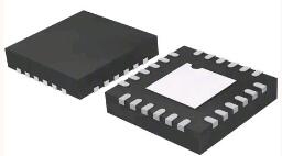
Details
BUY AD5700ACPZ https://www.utsource.net/itm/p/12612255.html
| Parameter | Symbol | Min | Typ | Max | Unit | Description |
|---|---|---|---|---|---|---|
| Supply Voltage | VDD | 2.7 | 3.3 | 5.5 | V | Power supply voltage |
| Output Current (Drive) | IOUT | - | 1 | 20 | mA | Maximum output current |
| Output Voltage Range | VOUT | 0 | - | VDD | V | Output voltage range |
| Input Voltage | VIN | 0 | - | VDD | V | Input voltage range |
| Operating Temperature | Toper | -40 | - | 85 | 掳C | Operating temperature range |
| Storage Temperature | Tstg | -65 | - | 150 | 掳C | Storage temperature range |
| Bandwidth | fBW | - | 10 | - | kHz | Small-signal bandwidth |
| Output Impedance | ZOUT | - | 1 | - | k惟 | Output impedance |
| Quiescent Current | IQ | - | 1 | - | mA | Quiescent current |
| Power Dissipation | PD | - | - | 15 | mW | Maximum power dissipation |
| Input Offset Voltage | VOS | -1 | 0 | 1 | mV | Input offset voltage |
| Common-Mode Rejection Ratio | CMRR | 80 | - | 100 | dB | Common-mode rejection ratio |
| Power-On Reset Time | tPOR | - | 100 | - | 渭s | Power-on reset time |
| Enable Time | tEN | - | 10 | - | 渭s | Time to enable the device after EN pin is high |
| Disable Time | tDIS | - | 10 | - | 渭s | Time to disable the device after EN pin is low |
Instructions for Using AD5700ACPZ
Power Supply:
- Connect the VDD pin to a stable power supply within the range of 2.7V to 5.5V.
- Ensure that the power supply has adequate filtering to minimize noise.
Output Configuration:
- The output voltage range is from 0V to VDD. Connect the load to the VOUT pin.
- Ensure the load resistance is appropriate to avoid excessive current draw.
Input Signal:
- Apply the input signal to the VIN pin. The input voltage should be within the range of 0V to VDD.
- Use a suitable input impedance to match the source.
Temperature Considerations:
- Operate the device within the temperature range of -40掳C to 85掳C for optimal performance.
- Store the device in an environment between -65掳C and 150掳C.
Power-On Reset:
- After applying power, the device will perform a power-on reset, which takes approximately 100 渭s.
Enable/Disable:
- To enable the device, set the EN pin high. The device will be enabled within 10 渭s.
- To disable the device, set the EN pin low. The device will be disabled within 10 渭s.
Noise and Interference:
- Use bypass capacitors close to the VDD and GND pins to reduce noise.
- Shield sensitive input and output lines to minimize interference.
Output Protection:
- Ensure the output is not short-circuited to prevent damage.
- Use external protection circuits if necessary to handle overvoltage or reverse polarity conditions.
Layout Considerations:
- Keep signal paths as short as possible to minimize parasitic effects.
- Use ground planes to improve thermal management and reduce noise.
Testing and Validation:
- Test the device under various operating conditions to ensure it meets the required specifications.
- Validate the design with the actual load and environmental conditions.
For detailed information, refer to the datasheet and application notes provided by Analog Devices.
(For reference only)View more about AD5700ACPZ on main site