
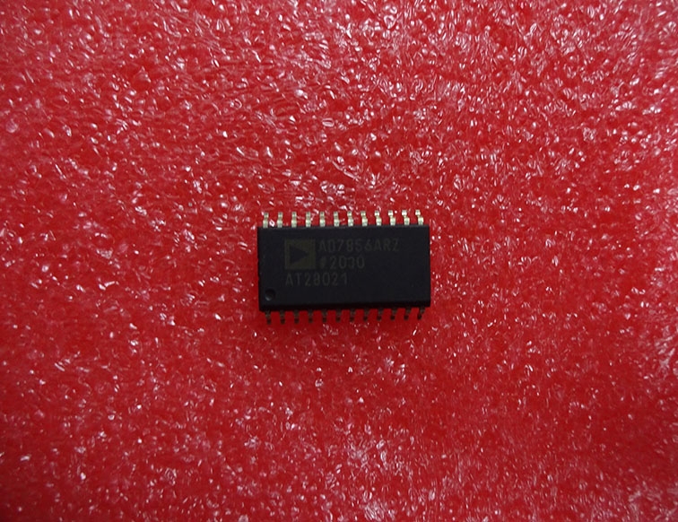
AD7856ARZ
Specifications
SKU
12612264
Details
BUY AD7856ARZ https://www.utsource.net/itm/p/12612264.html
| Parameter | Symbol | Conditions | Min | Typ | Max | Unit |
|---|---|---|---|---|---|---|
| Supply Voltage | VDD | 4.75 | 5.0 | 5.25 | V | |
| Analog Input Range | VIN | 0 | VDD | V | ||
| Conversion Time | tCONV | 100 kSPS | 10 | μs | ||
| Power Consumption | IDD | All channels on | 30 | mA | ||
| Output Data Rate | ODR | 100 | kSPS | |||
| Differential Nonlinearity | DNL | -1 | 0 | +1 | LSB | |
| Integral Nonlinearity | INL | -2 | 0 | +2 | LSB | |
| Signal-to-Noise Ratio | SNR | 100 kSPS | 78 | dB | ||
| Total Harmonic Distortion | THD | 100 kSPS | -85 | dB | ||
| Operating Temperature | Toper | -40 | 85 | °C | ||
| Storage Temperature | Tstg | -65 | 150 | °C |
Instructions for Using AD7856ARZ
Power Supply:
- Connect the supply voltage (VDD) to a stable 5V source.
- Ensure the power supply is clean and has low noise to avoid affecting the ADC performance.
Analog Inputs:
- Connect the analog inputs (VIN) within the range of 0V to VDD.
- Use differential inputs for better noise rejection and accuracy.
Conversion Control:
- Start a conversion by asserting the START pin.
- The conversion time is approximately 10 μs at 100 kSPS.
- Monitor the BUSY pin to determine when the conversion is complete.
Data Output:
- Read the conversion result from the data output pins (D0-D11).
- Use the CS (Chip Select) and RD (Read) signals to control data read operations.
Clocking:
- Provide an external clock signal to the CLK pin if using an external clock.
- The internal oscillator can also be used for clock generation.
Temperature Considerations:
- Operate the device within the temperature range of -40°C to 85°C.
- Store the device between -65°C and 150°C.
Handling and ESD Protection:
- Handle the device with care to avoid electrostatic discharge (ESD).
- Use proper grounding and ESD protection during handling and assembly.
Layout and Grounding:
- Use a ground plane to minimize noise and improve performance.
- Keep analog and digital grounds separate and connect them at a single point near the ADC.
Decoupling Capacitors:
- Place decoupling capacitors close to the power supply pins to filter out noise.
- Typical values are 0.1 μF and 10 μF.
Testing and Calibration:
- Perform initial testing with known input voltages to verify correct operation.
- Calibrate the ADC if necessary to achieve optimal performance.
For detailed specifications and advanced features, refer to the AD7856ARZ datasheet provided by Analog Devices.
(For reference only)View more about AD7856ARZ on main site