
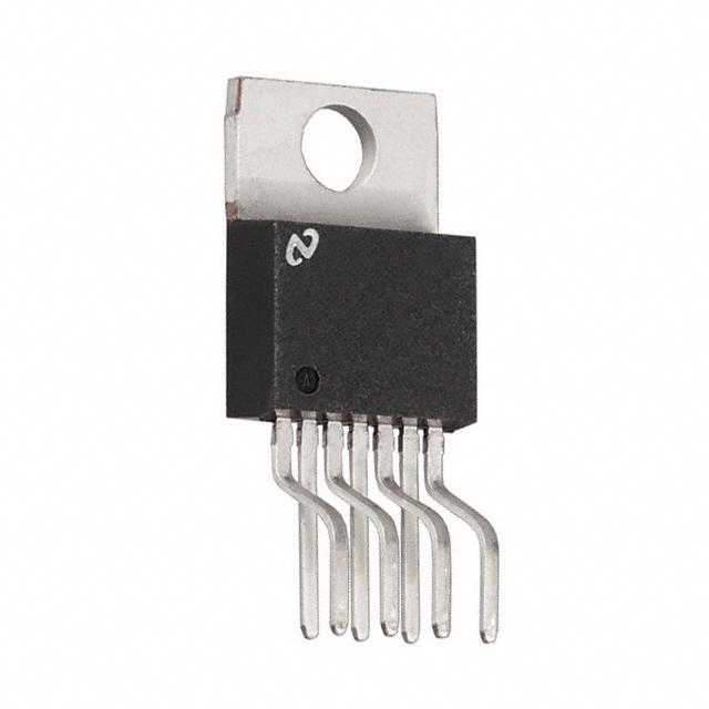
Details
BUY LM2678T-ADJ/NOPB https://www.utsource.net/itm/p/12612269.html
| Parameter | Symbol | Min | Typical | Max | Unit |
|---|---|---|---|---|---|
| Input Voltage | VIN | 4.5 | - | 36 | V |
| Output Voltage | VOUT | 1.23 | - | 35 | V |
| Output Current | IOUT | - | 3 | 5 | A |
| Switching Frequency | fSW | - | 260 | - | kHz |
| Efficiency | 畏 | - | 90 | - | % |
| Quiescent Current | IQ | - | 5 | - | mA |
| Shutdown Current | ISD | - | 50 | - | 渭A |
| Line Regulation | - | - | 0.01 | - | %/V |
| Load Regulation | - | - | 0.01 | - | %/A |
| Output Ripple Voltage | VRIPL | - | 100 | - | mVp-p |
| Thermal Resistance (胃JA) | - | - | 40 | - | 掳C/W |
Instructions for Using the LM2678T-ADJ/NOPB
Input Voltage (VIN):
- The input voltage should be within the range of 4.5V to 36V.
- Ensure that the input voltage is stable and does not exceed the maximum rating to avoid damaging the device.
Output Voltage (VOUT):
- The output voltage can be adjusted from 1.23V to 35V using external resistors.
- Use the formula ( V_ = 1.23 left(1 + fracright) ) to set the desired output voltage, where ( R_1 ) and ( R_2 ) are the feedback resistors.
Output Current (IOUT):
- The typical output current is 3A, with a maximum of 5A.
- Ensure that the load does not exceed the maximum output current to prevent overheating or damage.
Switching Frequency (fSW):
- The switching frequency is typically 260kHz.
- This frequency can be adjusted by changing the value of the external inductor and capacitor.
Efficiency (畏):
- The efficiency is typically around 90%.
- Optimize the efficiency by selecting appropriate components and ensuring good thermal management.
Quiescent Current (IQ):
- The quiescent current is typically 5mA.
- This current is drawn even when the device is not supplying any load.
Shutdown Current (ISD):
- The shutdown current is typically 50渭A.
- Use the shutdown pin to reduce power consumption when the device is not in use.
Line Regulation:
- The line regulation is typically 0.01%/V.
- This indicates how much the output voltage changes with variations in the input voltage.
Load Regulation:
- The load regulation is typically 0.01%/A.
- This indicates how much the output voltage changes with variations in the load current.
Output Ripple Voltage (VRIPL):
- The typical output ripple voltage is 100mV peak-to-peak.
- Use appropriate filtering components to minimize ripple if required.
Thermal Resistance (胃JA):
- The thermal resistance is typically 40掳C/W.
- Ensure adequate heat dissipation to keep the device temperature within safe limits.
Additional Notes:
- Always use proper PCB layout techniques to minimize noise and improve performance.
- Refer to the datasheet for detailed information on component selection and layout guidelines.
View more about LM2678T-ADJ/NOPB on main site