
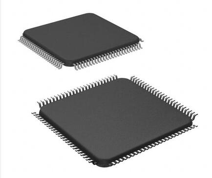
Details
BUY DS90CR483AVJD https://www.utsource.net/itm/p/12612275.html
| Parameter | Description | Min | Typ | Max | Unit |
|---|---|---|---|---|---|
| Supply Voltage (VCC) | Operating supply voltage | 2.7 | - | 5.5 | V |
| Operating Temperature | Temperature range for operation | -40 | - | 125 | 掳C |
| Data Rate | Maximum data rate | - | 200 | - | Mbps |
| Differential Output Swing | Differential output voltage swing | 360 | - | 600 | mV |
| Differential Input Threshold | Differential input threshold | 卤100 | - | 卤200 | mV |
| Propagation Delay | Time delay from input to output | - | 2.5 | - | ns |
| Skew | Maximum difference in propagation delay between channels | - | 0.5 | - | ns |
| Power Consumption | Typical power consumption at 200 Mbps | - | 100 | - | mW |
Instructions:
Power Supply:
- Ensure the supply voltage (VCC) is within the range of 2.7V to 5.5V.
- Use a stable power source to avoid fluctuations that could affect performance.
Temperature:
- Operate the device within the temperature range of -40掳C to 125掳C to ensure reliable performance.
- Avoid exposing the device to extreme temperatures outside this range.
Data Rate:
- The device supports a maximum data rate of 200 Mbps. Ensure the system clock and data signals are synchronized to achieve this rate.
Differential Signals:
- The differential output swing should be between 360 mV and 600 mV.
- The differential input threshold is 卤100 mV to 卤200 mV. Ensure the input signals meet these thresholds for proper operation.
Propagation Delay:
- The typical propagation delay is 2.5 ns. This value can be used for timing calculations in your design.
- The skew between channels should not exceed 0.5 ns to maintain signal integrity.
Power Consumption:
- The typical power consumption at 200 Mbps is 100 mW. Ensure the power supply can handle this load.
Layout and Grounding:
- Use proper PCB layout techniques to minimize noise and crosstalk.
- Ensure a solid ground plane and use decoupling capacitors close to the power pins to filter out noise.
Signal Integrity:
- Use controlled impedance traces for differential pairs to maintain signal integrity.
- Terminate differential lines with appropriate resistors to prevent reflections and signal degradation.
Testing:
- Verify the functionality of the device using a signal generator and oscilloscope.
- Test the device under various operating conditions to ensure robust performance.
View more about DS90CR483AVJD on main site