
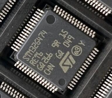
Details
BUY STM32G474RET6 https://www.utsource.net/itm/p/12612277.html
Below is the parameter table for the STM32G474RET6 microcontroller, followed by some basic instructions.
STM32G474RET6 Parameter Table
| Parameter | Value | Unit |
|---|---|---|
| Package | LQFP100 | |
| Operating Voltage (Vdd) | 1.7 to 3.6 | V |
| Core | ARM? Cortex?-M4 | |
| Clock Speed | Up to 170 | MHz |
| Flash Memory | 512 | KB |
| SRAM | 160 | KB |
| Temperature Range | -40 to 85 | 掳C |
| Analog-to-Digital Converters (ADCs) | 3 x 12-bit, 5 MSPS | |
| Digital-to-Analog Converters (DACs) | 2 x 12-bit | |
| Timers | 2 x 32-bit advanced control (TIM1, TIM8) 2 x 32-bit general-purpose (TIM2, TIM5) 4 x 16-bit general-purpose (TIM3, TIM4, TIM6, TIM7) 2 x 16-bit low-power (LPTIM1, LPTIM2) |
|
| Communication Interfaces | 2 x I2C 4 x USART 2 x SPI 1 x USB OTG FS 1 x SAI 1 x FDCAN |
|
| GPIO Pins | 80 | |
| Power Management | Low power modes: Sleep, Stop, Standby | |
| Capacitive Touch Sensing | Up to 24 channels | |
| CRC Calculation Unit | Yes | |
| True Random Number Generator (TRNG) | Yes | |
| DMA Channels | 16 | |
| Watchdog Timers | Independent WDT, Window WDT | |
| System Clock Sources | HSI (16 MHz), HSE (4 to 48 MHz), LSI (32 kHz), LSE (32.768 kHz) |
Basic Instructions for STM32G474RET6
Power Supply:
- Connect Vdd to the power supply (1.7 to 3.6V).
- Ensure Vss is connected to ground.
- Use decoupling capacitors (e.g., 100nF and 10uF) close to the power pins to stabilize the supply.
Clock Configuration:
- Configure the system clock using the internal HSI (16 MHz) or external HSE (4 to 48 MHz).
- Use the PLL to achieve the desired clock frequency (up to 170 MHz).
GPIO Initialization:
- Enable the GPIO clock in the RCC (Reset and Clock Control) register.
- Configure the GPIO mode (input, output, alternate function, analog).
- Set the output type (push-pull, open-drain).
- Configure the speed and pull-up/pull-down resistors.
Peripheral Initialization:
- Enable the peripheral clock in the RCC register.
- Configure the peripheral settings (e.g., baud rate for UART, prescaler for timers).
- Initialize the peripheral using the appropriate initialization functions.
Interrupt Handling:
- Enable the interrupt in the NVIC (Nested Vectored Interrupt Controller).
- Write the interrupt service routine (ISR) for the specific interrupt.
- Set the priority of the interrupt if necessary.
Low Power Modes:
- Enter low power modes (Sleep, Stop, Standby) using the PWR (Power Control) register.
- Configure the wake-up sources (e.g., EXTI lines, RTC alarms).
Flash Programming:
- Use the HAL (Hardware Abstraction Layer) library or direct register manipulation to program the flash memory.
- Ensure the flash write protection is configured correctly.
Debugging:
- Connect a debugger (e.g., ST-Link) to the SWD (Serial Wire Debug) interface.
- Use an IDE (e.g., STM32CubeIDE) to upload and debug the code.
For more detailed information, refer to the STM32G474RET6 datasheet and reference manual available on the STMicroelectronics website.
(For reference only)View more about STM32G474RET6 on main site