
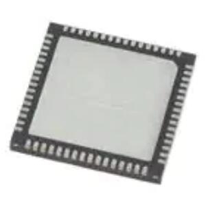
Details
BUY EFM32LG330F256G-E-QFN64 https://www.utsource.net/itm/p/12612283.html
| Parameter | Description | Value |
|---|---|---|
| Package | Package Type | QFN64 |
| Pins | Number of Pins | 64 |
| Operating Voltage (VDD) | Supply Voltage Range | 1.8V to 3.8V |
| Core | Microcontroller Core | ARM Cortex-M3 |
| Clock Speed | Maximum Clock Frequency | 48 MHz |
| Flash Memory | Flash Memory Size | 256 KB |
| RAM | RAM Size | 32 KB |
| Temperature Range | Operating Temperature Range | -40掳C to 85掳C |
| I/O Ports | Number of I/O Ports | 48 |
| ADC | Analog-to-Digital Converter Channels | 12-bit, 16 channels |
| DAC | Digital-to-Analog Converter Channels | 12-bit, 2 channels |
| Timers | Timers/Counters | 6 |
| Communication Interfaces | Supported Communication Interfaces | UART, SPI, I2C, USB |
| Watchdog Timer | Watchdog Timer | Yes |
| Low Power Modes | Low Power Modes | EM0, EM1, EM2, EM3 |
| Power Consumption | Active Mode Current (Typical) | 160 渭A/MHz |
| Package Dimensions | Package Dimensions (L x W x H) | 10 mm x 10 mm x 1 mm |
| ESD Protection | Electrostatic Discharge Protection | 卤2 kV (HBM) |
| Certifications | Regulatory Certifications | CE, FCC |
Instructions for Use
Power Supply:
- Ensure the supply voltage (VDD) is within the specified range of 1.8V to 3.8V.
- Use appropriate decoupling capacitors (typically 100nF and 10渭F) close to the power pins to stabilize the supply.
Clock Configuration:
- The internal oscillator can be used for basic applications. For more precise timing, an external crystal or clock source can be connected to the XIN and XOUT pins.
- Configure the system clock using the System Control Block (SCB) registers.
GPIO Configuration:
- Configure the I/O ports using the GPIO registers. Set the direction (input or output), pull-up/pull-down resistors, and drive strength as needed.
- Use the port configuration registers to enable or disable specific pins.
Peripheral Initialization:
- Initialize communication interfaces (UART, SPI, I2C, USB) by configuring the corresponding peripheral registers.
- Set up ADC and DAC channels by configuring the respective control registers and enabling the necessary clocks.
Low Power Modes:
- Enter low power modes (EM0, EM1, EM2, EM3) by configuring the appropriate registers in the Power Control Unit (PCU).
- Ensure that any active peripherals are properly managed during transitions between power modes.
Interrupt Handling:
- Set up interrupt vectors and enable interrupts in the Nested Vectored Interrupt Controller (NVIC).
- Write interrupt service routines (ISRs) to handle specific events.
Programming and Debugging:
- Use a JTAG or SWD debugger to program the flash memory and debug the application.
- Ensure the debug interface pins (TCK, TMS, TDI, TDO, SWDIO, SWCLK) are properly connected to the debugger.
ESD Protection:
- Handle the device with care to avoid electrostatic discharge.
- Use anti-static wrist straps and mats when handling the device.
Environmental Considerations:
- Store and operate the device within the specified temperature range to ensure reliable operation.
- Avoid exposure to excessive humidity and contaminants.
For detailed register descriptions and programming examples, refer to the EFM32LG330F256G datasheet and reference manual.
(For reference only)View more about EFM32LG330F256G-E-QFN64 on main site