
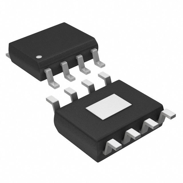
Details
BUY LMR33630BDDA https://www.utsource.net/itm/p/12612292.html
Below is the parameter table and instructions for the LMR33630BDDA, a 3.3V, 6A Synchronous Step-Down DC/DC Converter from Texas Instruments.
LMR33630BDDA Parameter Table
| Parameter | Symbol | Min | Typ | Max | Unit | Conditions |
|---|---|---|---|---|---|---|
| Input Voltage | VIN | 4.5 | - | 60 | V | |
| Output Voltage | VOUT | 0.8 | 3.3 | 17.5 | V | Adjustable with external resistors |
| Output Current | IOUT | - | 6 | - | A | Continuous output current |
| Switching Frequency | fSW | 200 | 2.1 | 2.2 | kHz/MHz | Adjustable with external resistor |
| Efficiency (Typical) | η | - | 94 | - | % | At 12V input, 3.3V output, 1A load |
| Quiescent Current | IQ | - | 50 | - | μA | No load, 12V input |
| Shutdown Current | ISD | - | 1 | - | μA | Shutdown mode |
| Start-Up Time | tSTART | - | 2.5 | - | ms | From 0V to 90% VOUT |
| Thermal Shutdown | TSD | - | 160 | - | °C | Junction temperature |
| Operating Temperature | TOPR | -40 | - | 125 | °C | Ambient temperature |
| Storage Temperature | TSTG | -65 | - | 150 | °C | |
| Package Type | - | - | - | - | 16-pin LLP | 3mm x 4mm |
Instructions for Using LMR33630BDDA
Input Capacitor (CIN):
- Place a ceramic capacitor (10μF to 22μF) close to the VIN and GND pins to filter out high-frequency noise.
- Additional bulk capacitance may be required for high-current applications.
Output Capacitor (COUT):
- Use a low ESR ceramic capacitor (10μF to 47μF) to stabilize the output voltage.
- For better transient response, consider using multiple capacitors in parallel.
Inductor Selection:
- Choose an inductor with a saturation current rating greater than the maximum output current.
- Typical inductance values range from 1.0μH to 4.7μH, depending on the switching frequency and output current.
Feedback Resistors (R1 and R2):
- Set the output voltage by adjusting the ratio of R1 and R2.
- Use the formula: VOUT = 0.8V * (1 + R1/R2)
- Example: For 3.3V output, use R1 = 10kΩ and R2 = 2.49kΩ.
Frequency Setting Resistor (RT):
- Adjust the switching frequency by connecting a resistor between the RT and GND pins.
- Use the formula: fSW = 2.1MHz / (1 + RT/10kΩ)
- Example: For 2.1MHz, use RT = 0Ω (short circuit).
Enable Pin (EN):
- The EN pin controls the on/off state of the converter.
- Apply a logic high (≥1.23V) to enable the converter.
- Apply a logic low (≤0.8V) to disable the converter and enter shutdown mode.
Thermal Management:
- Ensure adequate PCB copper area for heat dissipation.
- Use thermal vias to transfer heat to the bottom layer or heat sink if necessary.
Layout Considerations:
- Keep the input and output capacitors as close as possible to the IC.
- Minimize trace lengths and widths for high-frequency signals.
- Use a ground plane to reduce noise and improve stability.
Protection Features:
- The LMR33630BDDA includes overcurrent protection, thermal shutdown, and undervoltage lockout (UVLO) to protect the device from damage.
By following these instructions, you can ensure optimal performance and reliability of the LMR33630BDDA in your design.
(For reference only)View more about LMR33630BDDA on main site