
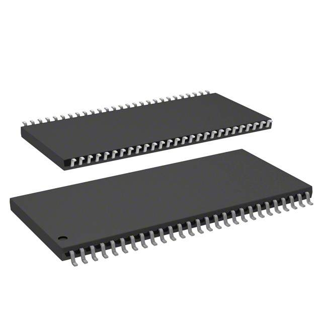
Details
BUY IS42S16320F-6TL https://www.utsource.net/itm/p/12612298.html
| Parameter | Description | Value |
|---|---|---|
| Device Type | 32 M-Bit (4M x 8, 2M x 16, 1M x 32) Synchronous DRAM | - |
| Organization | 4 Banks | - |
| Data Width | 8/16/32 bits | - |
| Supply Voltage (Vcc) | Operating Range | 2.25 V to 3.6 V |
| Supply Voltage (Vccq) | I/O Power Supply | 2.25 V to 3.6 V |
| Operating Temperature | Commercial | 0掳C to 70掳C |
| Industrial | -40掳C to 85掳C | |
| Access Time (tAC) | - | 6 ns |
| CAS Latency (CL) | - | 2, 3 |
| RAS# to CAS# Delay (tRCD) | - | 2, 3 cycles |
| Row Active to Precharge Delay (tRAS) | - | 5, 6 cycles |
| Refresh Cycle Time (tREF) | - | 64 ms (8192 refresh cycles) |
| Write Recovery Time (tWR) | - | 2 cycles |
| Exit Self-Refresh to Access Time (tXSR) | - | 75 ns |
| Power Down Exit Time (tXP) | - | 20 ns |
| Package Type | - | BGA (Ball Grid Array) |
| Pin Count | - | 48 pins |
Instructions for Use:
Power Supply:
- Ensure that both Vcc and Vccq are within the specified operating range (2.25 V to 3.6 V).
- Use decoupling capacitors close to the power supply pins to reduce noise and ensure stable operation.
Temperature Considerations:
- Operate the device within the specified temperature range for commercial (0掳C to 70掳C) or industrial (-40掳C to 85掳C) applications.
Timing Parameters:
- Adhere to the specified access time (tAC) of 6 ns.
- Set the CAS latency (CL) to either 2 or 3 cycles.
- Ensure the RAS# to CAS# delay (tRCD) is set to 2 or 3 cycles.
- The row active to precharge delay (tRAS) should be 5 or 6 cycles.
- Maintain a refresh cycle time (tREF) of 64 ms with 8192 refresh cycles.
- Set the write recovery time (tWR) to 2 cycles.
- Ensure the exit self-refresh to access time (tXSR) is at least 75 ns.
- The power-down exit time (tXP) should be 20 ns.
Initialization:
- After power-up, perform a mode register set (MRS) command to initialize the device.
- Set the mode register according to the desired operating parameters (e.g., CAS latency, burst length).
Memory Operations:
- Use the appropriate control signals (RAS#, CAS#, WE#, etc.) to perform read, write, and refresh operations.
- Ensure that the address lines are correctly driven during memory access.
Self-Refresh Mode:
- Enter self-refresh mode by asserting the self-refresh request signal.
- To exit self-refresh mode, deassert the self-refresh request signal and wait for the tXSR period before accessing the memory.
Power Management:
- Use the power-down mode to reduce power consumption when the device is not in use.
- To exit power-down mode, deassert the power-down signal and wait for the tXP period before accessing the memory.
Package Handling:
- Handle the BGA package with care to avoid damage to the balls.
- Follow recommended soldering and reflow profiles to ensure reliable bonding.
For detailed information and specific application notes, refer to the datasheet provided by the manufacturer.
(For reference only)View more about IS42S16320F-6TL on main site