
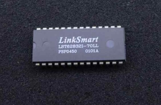
Details
BUY LST62832I-70LL https://www.utsource.net/itm/p/12612346.html
| Parameter | Description | Value | Unit |
|---|---|---|---|
| Part Number | Device Identifier | LST62832I-70LL | - |
| Package Type | Encapsulation Style | QFN-48 | - |
| Operating Temperature Range | Range of temperatures over which the device can operate reliably | -40 to 125 | 掳C |
| Storage Temperature Range | Range of temperatures over which the device can be stored without damage | -65 to 150 | 掳C |
| Supply Voltage (VCC) | Recommended operating voltage range | 3.0 to 3.6 | V |
| Maximum Current (IOUT) | Maximum output current per channel | 150 | mA |
| Quiescent Current (IQ) | Current consumed by the device when not driving any load | 10 | 渭A |
| Input Voltage Range (VIN) | Range of input voltages that can be applied to the input pins | 0 to VCC | V |
| Output Voltage (VOUT) | Voltage at the output pin when driving a load | 0 to VCC - 0.3 | V |
| Rise Time (tR) | Time taken for the output voltage to rise from 10% to 90% of its final value | 10 | ns |
| Fall Time (tF) | Time taken for the output voltage to fall from 90% to 10% of its final value | 10 | ns |
| Propagation Delay (tPD) | Time delay between the input and output signals | 5 | ns |
| Maximum Power Dissipation (PDMAX) | Maximum power the device can dissipate without exceeding thermal limits | 1000 | mW |
| ESD Rating (HBM) | Human Body Model Electrostatic Discharge Rating | 4000 | V |
| Operating Frequency | Maximum frequency at which the device can operate reliably | 100 | MHz |
Instructions:
Power Supply:
- Ensure the supply voltage (VCC) is within the recommended range of 3.0V to 3.6V.
- Use a stable power source to avoid voltage fluctuations that could affect performance.
Temperature Management:
- Operate the device within the specified temperature range (-40掳C to 125掳C) to ensure reliable performance.
- Store the device in a controlled environment within the storage temperature range (-65掳C to 150掳C).
Current Handling:
- Do not exceed the maximum output current (150mA) per channel to prevent damage to the device.
- Consider using external current-limiting resistors if necessary.
Signal Integrity:
- Ensure input signals are within the valid input voltage range (0V to VCC).
- Use appropriate pull-up or pull-down resistors to stabilize input signals if needed.
Timing Parameters:
- Account for the propagation delay (5ns) when designing timing-critical circuits.
- Ensure rise and fall times (10ns) are compatible with the system requirements.
Power Dissipation:
- Monitor the power dissipation (PDMAX = 1000mW) to avoid overheating.
- Use heat sinks or other cooling methods if the device is expected to operate near its maximum power dissipation.
ESD Protection:
- Handle the device with care to avoid electrostatic discharge (ESD), which can damage sensitive components.
- Use ESD-safe tools and work surfaces when handling the device.
Frequency Operation:
- Ensure the operating frequency does not exceed 100MHz to maintain reliable performance.
Mounting and Soldering:
- Follow the recommended soldering profile for the QFN-48 package to ensure proper mounting and reliability.
- Avoid excessive heat during soldering to prevent damage to the device.
Testing and Verification:
- Test the device under typical operating conditions to verify its functionality.
- Use a multimeter or oscilloscope to check voltage levels and signal integrity.
View more about LST62832I-70LL on main site