
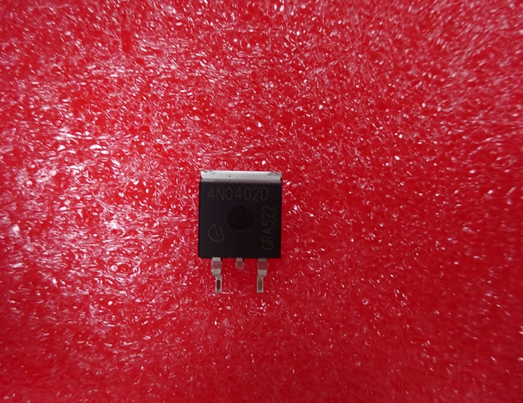
Details
BUY 4N0402D https://www.utsource.net/itm/p/12612378.html
| Parameter | Symbol | Min | Typ | Max | Unit | Description |
|---|---|---|---|---|---|---|
| Input Voltage | VI | -0.3 | - | 5.5 | V | Maximum voltage that can be applied to the input pin. |
| Output Voltage | VO | -0.3 | - | 5.5 | V | Maximum voltage that can be applied to the output pin. |
| Continuous Current | IC | - | - | 100 | mA | Maximum continuous current through the device. |
| Peak Current | IPK | - | - | 200 | mA | Maximum peak current through the device. |
| Power Dissipation | PD | - | - | 625 | mW | Maximum power dissipation at 25掳C ambient temperature. |
| Operating Temperature | TA | -40 | - | 85 | 掳C | Ambient operating temperature range. |
| Storage Temperature | TSTG | -65 | - | 150 | 掳C | Temperature range for storage. |
| Junction Temperature | TJ | - | - | 150 | 掳C | Maximum junction temperature. |
Instructions:
Power Supply:
- Ensure the input voltage (VI) and output voltage (VO) do not exceed their respective maximum ratings.
Current Handling:
- Do not exceed the continuous current (IC) or peak current (IPK) ratings to avoid damage to the device.
Power Dissipation:
- Ensure the power dissipation (PD) does not exceed the maximum rating, especially in high-temperature environments.
Temperature Management:
- Operate the device within the specified ambient temperature (TA) and storage temperature (TSTG) ranges.
- Monitor the junction temperature (TJ) to prevent overheating.
Handling and Storage:
- Handle the device with care to avoid mechanical damage.
- Store the device in a dry environment within the specified storage temperature range.
Soldering:
- Use appropriate soldering techniques and ensure the device is not exposed to excessive heat during soldering.
Testing:
- Perform all tests within the specified operating conditions to ensure reliable performance.
View more about 4N0402D on main site