
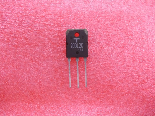
Details
BUY 20DL2C https://www.utsource.net/itm/p/12612388.html
| Parameter | Description | Value |
|---|---|---|
| Part Number | Device Identifier | 20DL2C |
| Type | Device Type | CMOS Logic IC |
| Function | Logic Function | Dual 4-Input AND |
| Supply Voltage | Operating Voltage Range | 2V to 6V |
| Input Voltage | Maximum Input Voltage | Vcc + 0.5V |
| Output Voltage | Maximum Output Voltage (High Level) | Vcc - 0.1V |
| Output Current | Maximum Output Current (Sink) | 10mA |
| Propagation Delay | Typical Propagation Delay Time | 10ns |
| Operating Temperature | Temperature Range for Operation | -40掳C to 85掳C |
| Storage Temperature | Temperature Range for Storage | -65掳C to 150掳C |
| Package | Encapsulation Type | SOIC-14 |
| Pin Count | Number of Pins | 14 |
Instructions:
Power Supply Connection:
- Connect Vcc (pin 14) to the positive supply voltage (2V to 6V).
- Connect GND (pin 7) to the ground.
Input Connections:
- Connect the inputs (pins 1, 2, 3, 4, 9, 10, 11, 12) to the desired logic levels (0V or Vcc).
Output Connections:
- The outputs (pins 5, 13) will provide the logical AND of the respective input groups.
- Ensure that the output is connected to a load that does not exceed the maximum output current (10mA).
Handling Precautions:
- Handle the IC with care to avoid static damage.
- Ensure that all connections are secure and within the specified voltage ranges.
- Do not exceed the maximum operating temperature range to prevent damage to the device.
Testing:
- Apply the appropriate logic levels to the inputs and verify the output using a multimeter or oscilloscope.
- Check for correct operation by comparing the output with the expected logical AND function results.
View more about 20DL2C on main site