
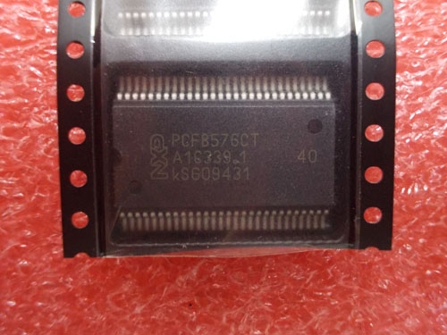
Details
BUY PCF8576CT https://www.utsource.net/itm/p/12612394.html
| Parameter | Symbol | Min | Typical | Max | Unit | Description |
|---|---|---|---|---|---|---|
| Supply Voltage | VCC | 2.0 | - | 6.0 | V | Operating voltage range |
| Operating Temperature | TOP | -40 | - | 85 | 掳C | Temperature range for normal operation |
| Storage Temperature | TSTG | -65 | - | 150 | 掳C | Temperature range for storage |
| I2C Bus Speed | fSCL | - | 100 | 400 | kHz | Maximum clock frequency of the I2C bus |
| Input Current (High) | IINH | - | 0.01 | 0.4 | mA | Input current when the input is high |
| Input Current (Low) | IINL | - | 0.01 | 0.4 | mA | Input current when the input is low |
| Output Current (High) | IOH | - | 0.4 | 3.2 | mA | Output current when the output is high |
| Output Current (Low) | IOL | 10 | 15 | 20 | mA | Output current when the output is low |
| Quiescent Current | IQ | 0.1 | 0.5 | 1.0 | mA | Current consumption in quiescent state |
| Leakage Current | ILK | - | 0.01 | 0.1 | 渭A | Leakage current at the output pins |
| Propagation Delay Time | tpd | 100 | 200 | 300 | ns | Time delay from input to output |
| Setup Time | tsu | 200 | 300 | 400 | ns | Minimum time before the clock edge that the data must be stable |
| Hold Time | th | 50 | 100 | 150 | ns | Minimum time after the clock edge that the data must be stable |
| I2C Address | A0-A2 | - | - | - | - | Address selection pins (0 to 7) |
Instructions for Using the PCF8576CT
Power Supply:
- Connect the VCC pin to a power supply within the range of 2.0V to 6.0V.
- Ensure the GND pin is connected to the ground.
I2C Bus Connection:
- Connect the SDA (Serial Data) and SCL (Serial Clock) pins to the I2C bus.
- Use pull-up resistors on both SDA and SCL lines to VCC. Typical values are 4.7k惟 to 10k惟.
Address Configuration:
- The device address can be configured using the A0, A1, and A2 pins. These pins can be tied to either VCC or GND to set the address.
- The default address is 0x38 (binary 0111000) if all address pins are grounded.
Communication Protocol:
- The PCF8576CT follows the standard I2C protocol.
- Start by sending the device address followed by a write command (0 for writing, 1 for reading).
- For writing, send the data byte(s) after the address.
- For reading, send the device address followed by a read command, then read the data byte(s).
Timing Considerations:
- Ensure the setup and hold times for data are respected to avoid communication errors.
- The propagation delay time should be considered when designing the system timing.
Output Configuration:
- The output pins can source or sink current as specified in the table.
- Ensure the load connected to the output pins does not exceed the maximum current ratings.
Operating Temperature:
- The device is designed to operate within the temperature range of -40掳C to 85掳C.
- Store the device within the storage temperature range of -65掳C to 150掳C.
Quiescent Current:
- The device consumes a quiescent current of up to 1.0mA, which should be considered in power budgeting.
Leakage Current:
- Be aware of the leakage current at the output pins, which can affect the performance of sensitive circuits.
Handling Precautions:
- Handle the device with care to avoid static damage.
- Follow proper soldering techniques to ensure reliable connections.
By following these instructions, you can effectively integrate the PCF8576CT into your circuit design.
(For reference only)View more about PCF8576CT on main site