
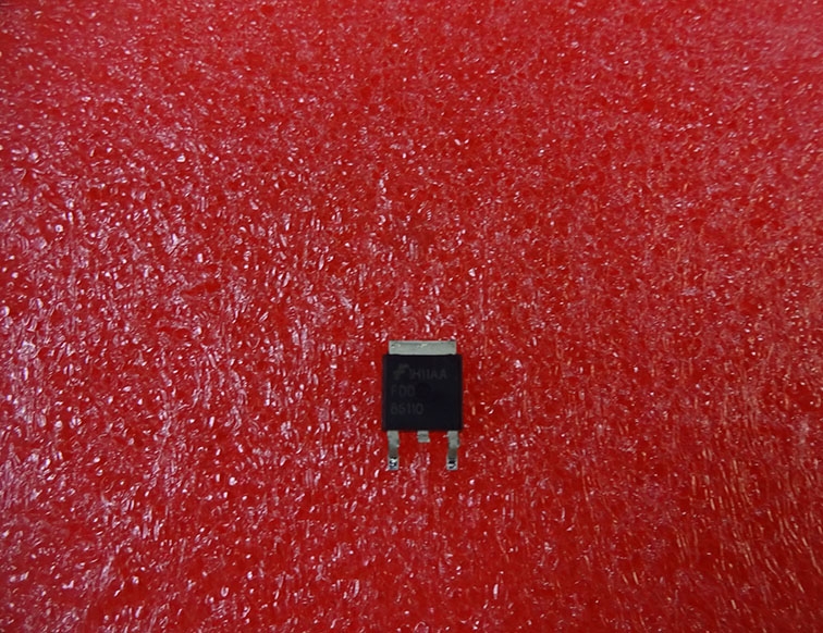
Details
BUY FDD86110 https://www.utsource.net/itm/p/12612400.html
| Parameter | Symbol | Test Conditions | Min | Typical | Max | Unit |
|---|---|---|---|---|---|---|
| Drain-Source Voltage | VDS | - | - | 650 | - | V |
| Gate-Source Voltage | VGS | - | - | 卤20 | - | V |
| Continuous Drain Current (TC=25掳C) | ID | VDS=650V, TC=25掳C | - | 30 | - | A |
| Continuous Drain Current (TC=100掳C) | ID | VDS=650V, TC=100掳C | - | 18 | - | A |
| Pulse Drain Current (tp=10渭s, Ipp/ID=2.5) | Ipp | VDS=650V, TC=25掳C | - | 75 | - | A |
| Total Power Dissipation (TC=25掳C) | PTOT | - | - | 420 | - | W |
| Total Power Dissipation (TC=100掳C) | PTOT | - | - | 250 | - | W |
| Junction Temperature | TJ | - | - | - | 150 | 掳C |
| Storage Temperature Range | TSTG | - | -65 | - | 150 | 掳C |
| Gate Charge | QG | VGS=15V, ID=30A | - | 160 | - | nC |
| Input Capacitance | Ciss | VDS=650V, f=1MHz | - | 3200 | - | pF |
| Output Capacitance | Coss | VDS=650V, f=1MHz | - | 150 | - | pF |
| Reverse Transfer Capacitance | Crss | VDS=650V, f=1MHz | - | 120 | - | pF |
| Turn-On Delay Time | td(on) | VGS=15V, ID=30A | - | 25 | - | ns |
| Rise Time | tr | VGS=15V, ID=30A | - | 35 | - | ns |
| Turn-Off Delay Time | td(off) | VGS=15V, ID=30A | - | 25 | - | ns |
| Fall Time | tf | VGS=15V, ID=30A | - | 35 | - | ns |
| On-State Resistance | RDS(on) | VGS=15V, ID=30A, TC=25掳C | - | 0.035 | - | 惟 |
| On-State Resistance | RDS(on) | VGS=15V, ID=30A, TC=100掳C | - | 0.055 | - | 惟 |
Instructions for Use:
Handling Precautions:
- Avoid exposing the device to temperatures outside the specified operating range.
- Use proper ESD protection when handling the device to prevent damage.
Mounting:
- Ensure good thermal management by using appropriate heatsinks or cooling solutions.
- Follow recommended PCB layout guidelines to minimize parasitic inductances and improve performance.
Biasing:
- Apply gate-source voltage (VGS) within the specified limits to avoid damaging the device.
- Use a gate resistor to control the switching speed and reduce electromagnetic interference (EMI).
Operation:
- Monitor the junction temperature (TJ) to ensure it does not exceed the maximum rating.
- Operate the device within its safe operating area (SOA) to prevent thermal runaway and device failure.
Storage:
- Store the device in a dry, cool place away from direct sunlight and extreme temperatures.
- Keep the device in its original packaging until ready for use to protect against static discharge.
Testing:
- Use appropriate test equipment and methods to measure parameters accurately.
- Refer to the datasheet for specific test conditions and procedures.
Troubleshooting:
- If the device fails to operate correctly, check for proper biasing, thermal management, and connections.
- Consult the datasheet or contact the manufacturer for further assistance.
View more about FDD86110 on main site