
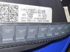
Details
BUY LV13605TJ-ADJ https://www.utsource.net/itm/p/12612434.html
| Parameter | Symbol | Min | Typ | Max | Unit | Description |
|---|---|---|---|---|---|---|
| Input Voltage | VIN | 2.7 | - | 5.5 | V | Operating input voltage range |
| Output Voltage | VOUT | - | - | 3.3 | V | Adjustable output voltage |
| Quiescent Current | IQ | - | 1.8 | - | 渭A | Supply current in normal operation |
| Shutdown Current | ISD | - | 0.1 | - | 渭A | Supply current in shutdown mode |
| Load Regulation | - | - | 0.4 | - | % | Change in output voltage for load currents from 0 to 200mA |
| Line Regulation | - | - | 0.2 | - | %/V | Change in output voltage for a change in input voltage |
| Dropout Voltage | VDROPOUT | - | 250 | - | mV | Maximum input-output differential voltage at full load |
| Operating Temperature | Toper | -40 | - | 85 | 掳C | Operating ambient temperature range |
| Storage Temperature | Tstg | -65 | - | 150 | 掳C | Storage temperature range |
Instructions:
- Input Voltage Setup: Ensure the input voltage is within the specified range of 2.7V to 5.5V.
- Output Voltage Adjustment: Adjust the output voltage using external resistors according to the formula provided in the datasheet.
- Quiescent and Shutdown Current Management: The device has low quiescent and shutdown currents, making it suitable for battery-operated applications. Use the shutdown pin to control power consumption.
- Load and Line Regulation: For optimal performance, ensure that changes in load or input voltage do not exceed the specified regulation percentages.
- Dropout Voltage Consideration: Keep the input voltage sufficiently above the output voltage to stay within the dropout voltage limit.
- Temperature Range: Operate the device within the specified temperature ranges to ensure reliability and longevity.
- Installation: Follow standard PCB layout guidelines for low-noise and stable operation. Place bypass capacitors close to the input and output pins.
View more about LV13605TJ-ADJ on main site