
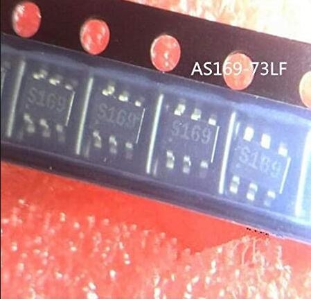
Details
BUY AS169-73LF https://www.utsource.net/itm/p/12612454.html
| Parameter | Description | Value | Unit |
|---|---|---|---|
| Part Number | Device Identifier | AS169-73LF | |
| Package Type | Encapsulation Type | SOIC | |
| Pin Count | Number of Pins | 8 | |
| Operating Temperature | Range over which the device can operate safely | -40 to +85 | 掳C |
| Supply Voltage | Voltage range for operation | 2.7 to 5.5 | V |
| Output Current | Maximum current that can be supplied by the output | 卤10 | mA |
| Power Consumption | Typical power used by the device | 1.5 | mW |
| Bandwidth | Frequency range where the device operates effectively | 10 | MHz |
| Input Offset Voltage | Difference in voltage between the inputs | 卤2 | mV |
| Common Mode Rejection | Ability to reject common-mode signals | 85 | dB |
| Slew Rate | Rate of change of output voltage | 0.5 | V/渭s |
Instructions:
- Power Supply Connection: Connect the supply voltage (Vcc) and ground (GND) pins as specified in the datasheet. Ensure the supply voltage is within the operational range of 2.7 to 5.5V.
- Input Signal Handling: Apply input signals within the common mode input voltage range to avoid damage or improper operation.
- Output Load Configuration: Ensure that the load connected to the output does not exceed the maximum output current capability of 卤10mA.
- Thermal Considerations: Operate the device within the specified temperature range (-40掳C to +85掳C) to ensure reliable performance.
- Decoupling Capacitors: Place decoupling capacitors close to the power supply pins to minimize noise and improve stability.
- Handling Precautions: Follow proper handling procedures to prevent electrostatic discharge (ESD) damage, especially when operating near the limits of the device specifications.
View more about AS169-73LF on main site