
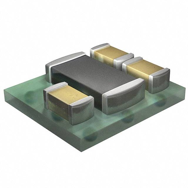
Details
BUY TPS81256SIPT https://www.utsource.net/itm/p/12612471.html
| Parameter | Symbol | Min | Typ | Max | Unit | Notes |
|---|---|---|---|---|---|---|
| Input Voltage | VIN | 2.7 | - | 5.5 | V | Operating range |
| Output Voltage | VOUT | - | 3.3 | - | V | Fixed output voltage |
| Output Current | IOUT | - | 500 | - | mA | Continuous output current |
| Efficiency | η | - | 90 | - | % | Typical efficiency at nominal conditions |
| Quiescent Current | IQ | - | 40 | - | μA | Typical quiescent current |
| Shutdown Current | ISD | - | 0.1 | - | μA | Typical shutdown current |
| Operating Temperature Range | TOPR | -40 | - | 125 | °C | Storage and operating temperature range |
| Junction Temperature | TJ | -40 | - | 150 | °C | Maximum junction temperature |
| Thermal Resistance (θJA) | θJA | - | 50 | - | °C/W | Typical thermal resistance to ambient |
| Start-Up Time | tSTARTUP | - | 200 | - | μs | Typical start-up time from enable to full output |
| Dropout Voltage | VDROPOUT | - | 250 | - | mV | Typical dropout voltage at full load |
| Enable Voltage (High) | VEN(HIGH) | 1.1 | - | 1.4 | V | Minimum enable voltage for high state |
| Enable Voltage (Low) | VEN(LOW) | - | 0.4 | 0.8 | V | Maximum enable voltage for low state |
| Reverse Input Protection | VREVIN | -5 | - | 5 | V | Maximum reverse input voltage |
| Output Voltage Accuracy | ΔVOUT | -1 | 0 | 1 | % | Output voltage accuracy over line and load |
Instructions for Use
Power Supply Connection:
- Connect the input voltage (VIN) to the positive terminal of the power supply.
- Connect the ground (GND) to the negative terminal of the power supply.
Output Connection:
- Connect the output voltage (VOUT) to the load.
- Ensure the load does not exceed the maximum output current (IOUT).
Enable Pin:
- To enable the device, apply a voltage greater than VEN(HIGH) to the enable pin.
- To disable the device, apply a voltage less than VEN(LOW) to the enable pin.
Thermal Management:
- Ensure adequate heat dissipation to keep the junction temperature (TJ) within the specified range.
- Use a heatsink if necessary, especially under high load conditions.
Capacitor Selection:
- Use a ceramic capacitor with low ESR for input and output filtering.
- Recommended values: 1 μF for input and 1 μF for output.
Reverse Voltage Protection:
- The device has built-in reverse voltage protection up to VREVIN.
- Avoid exceeding this limit to prevent damage.
Storage and Operating Temperature:
- Store and operate the device within the specified temperature range (TOPR and TJ) to ensure reliable performance.
Start-Up Time:
- The device will take approximately tSTARTUP to reach full output after being enabled.
Efficiency:
- The typical efficiency is given at nominal conditions. Actual efficiency may vary depending on input voltage, output load, and environmental conditions.
Output Voltage Accuracy:
- The output voltage will remain within ±1% of the nominal value under varying line and load conditions.
For detailed application circuits and further information, refer to the datasheet provided by the manufacturer.
(For reference only)View more about TPS81256SIPT on main site