
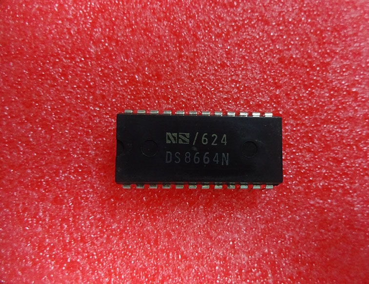
Details
BUY DS8664N https://www.utsource.net/itm/p/12617391.html
| Parameter | Description | DS8664N Value |
|---|---|---|
| Device Type | Description of the device type | Quad SPDT Analog Switch |
| Supply Voltage (Vcc) | Operating supply voltage range | 2.7V to 5.5V |
| On Resistance (Ron) | Resistance when switch is on | 10惟 max |
| Off Isolation | Isolation between input and output when switch is off | -75dB @ 1MHz |
| Propagation Delay | Time delay for signal propagation through the switch | 2ns max |
| Power Dissipation | Maximum power dissipation | 375mW |
| Operating Temperature | Range of temperatures in which the device can operate effectively | -40掳C to +85掳C |
| Package | Physical package type | SOIC-16, TSSOP-16 |
Instructions for Use:
- Power Supply: Ensure that the supply voltage (Vcc) is within the specified range of 2.7V to 5.5V.
- Signal Level: The input signals should be compatible with the supply voltage to prevent damage or improper operation.
- Control Inputs: Apply control signals to select the desired switch configuration (SPDT settings).
- Installation: Install the DS8664N in a suitable PCB layout ensuring proper thermal management, especially considering its maximum power dissipation of 375mW.
- Handling Precautions: Handle the component with care to avoid electrostatic discharge (ESD) damage; follow standard ESD handling procedures.
- Testing: After installation, test the device under typical operating conditions to ensure it meets performance specifications such as on-resistance and off-isolation.
View more about DS8664N on main site