
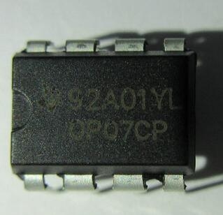
Details
BUY OP-07DP https://www.utsource.net/itm/p/12618312.html
| Parameter | Symbol | Conditions | Min | Typ | Max | Unit |
|---|---|---|---|---|---|---|
| Input Offset Voltage | VIO | Initial | -50 | 10 | 50 | μV |
| Input Bias Current | IB | -200 | 8 | 200 | nA | |
| Input Offset Current | IOS | -50 | 2 | 50 | nA | |
| Open Loop Gain | Avo | f = 0.1 Hz | 300 | 700 | kV/V | |
| Supply Voltage Range | VCC | ±2 | ±15 | V | ||
| Operating Temperature | Temp | Commercial, Industrial | 0 | 70 | °C | |
| Military | -55 | 125 | °C | |||
| Output Voltage Swing | VOS | IOL = 10 mA | ±12 | ±14 | V | |
| Slew Rate | SR | 0.13 | V/μs | |||
| Common Mode Rejection | CMRR | f = 0.1 Hz | 90 | 110 | dB | |
| Power Supply Rejection | PSRR | f = 0.1 Hz | 86 | 100 | dB | |
| Equivalent Input Noise | en | f = 1 kHz | 3 | nV/√Hz |
Instructions for OP-07DP
Power Supply Connections:
- Connect the positive supply voltage to pin 8 and the negative supply voltage to pin 4.
- Ensure that the supply voltages are within the specified range (±2V to ±15V).
Input Connections:
- Non-inverting input is connected to pin 3.
- Inverting input is connected to pin 2.
- Keep input signals within the common mode input voltage range.
Output Connections:
- The output is taken from pin 6.
- Ensure load resistance is appropriate to avoid excessive current draw.
Offset Nulling:
- For applications requiring minimal offset voltage, use the offset null pins (1 and 5).
- Connect a potentiometer between these pins with its wiper grounded for adjustment.
Decoupling Capacitors:
- Place decoupling capacitors close to the power supply pins to reduce noise and improve stability.
- Recommended values are typically 0.1 μF and 10 μF in parallel.
Operating Temperature:
- Ensure the device operates within the specified temperature range for reliable performance.
- Use heatsinks or other cooling methods if necessary for high-power applications.
Handling Precautions:
- Handle with care as ESD can damage the device.
- Follow proper anti-static procedures during handling and installation.
Testing:
- Before final assembly, test the operational amplifier in a known good circuit to ensure it functions correctly.
- Verify all connections and component values meet the design specifications.
View more about OP-07DP on main site