
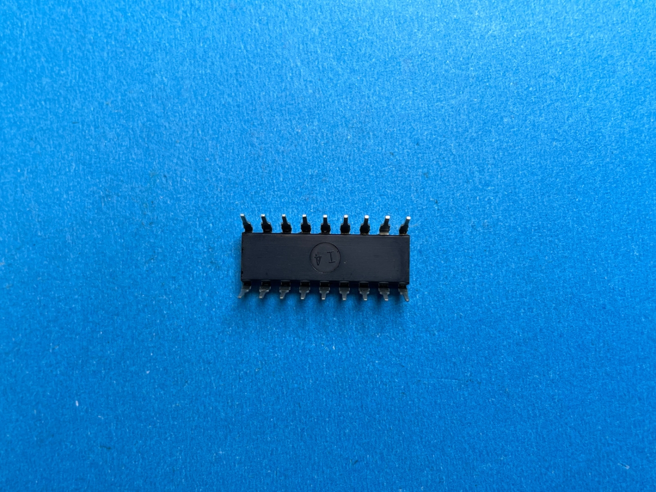
Details
BUY AN6891 https://www.utsource.net/itm/p/12618634.html
| Parameter | Description | Value |
|---|---|---|
| Part Number | Component Identifier | AN6891 |
| Function | Device Functionality | High-Efficiency Buck Converter |
| Input Voltage Range | Range of Input Voltage for Operation | 4.5V to 28V |
| Output Voltage Range | Range of Output Voltage Adjustable | 0.8V to 18V |
| Output Current | Maximum Continuous Output Current | 3A |
| Switching Frequency | Frequency at Which the Converter Operates | 500kHz to 2MHz |
| Quiescent Current | Current Drawn by the Device in Standby Mode | 25渭A (Typical) |
| Efficiency | Typical Efficiency at Rated Load | Up to 95% |
| Package Type | Physical Enclosure of the Device | QFN-16 (4x4mm) |
| Operating Temperature Range | Temperature Range for Reliable Operation | -40掳C to +125掳C |
| Storage Temperature Range | Temperature Range for Storage | -65掳C to +150掳C |
| Protection Features | Built-in Safety Mechanisms | Overcurrent, Overvoltage, Thermal Shutdown |
Instructions for Use
Power Supply Connection:
- Connect the input voltage to the VIN pin.
- Ensure the input voltage is within the specified range (4.5V to 28V).
Output Configuration:
- Set the output voltage using the feedback resistor network connected to the FB pin.
- Refer to the datasheet for specific resistor values based on desired output voltage.
Inductor Selection:
- Choose an inductor with a value that matches the switching frequency and output current requirements.
- Ensure the inductor has a saturation current rating higher than the maximum output current.
Capacitor Selection:
- Use input and output capacitors to stabilize the power supply and reduce ripple.
- Recommended input capacitance: 10渭F to 47渭F ceramic capacitor.
- Recommended output capacitance: 10渭F to 100渭F ceramic capacitor.
Thermal Management:
- Ensure adequate heat dissipation by providing a thermal path from the device to a heatsink or PCB plane.
- Use thermal vias to connect the exposed pad to a ground plane for better thermal performance.
Layout Considerations:
- Keep the traces between the input capacitor, inductor, and IC as short as possible to minimize parasitic inductance.
- Place the output capacitor close to the IC to reduce output ripple.
Protection Circuits:
- The AN6891 includes built-in overcurrent, overvoltage, and thermal shutdown protection.
- No additional external protection circuits are typically required unless specified by the application.
Testing and Validation:
- After assembly, test the converter under various load conditions to ensure stable operation and correct output voltage.
- Monitor the temperature of the device to ensure it stays within the operating temperature range.
View more about AN6891 on main site