
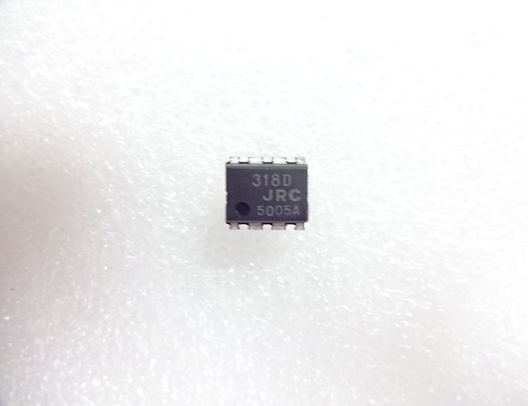
NJM318D
Category: Elec-componentLinear - Amplifiers - Instrumentation, OP Amps, Buffer AmpsIntegrated CircuitAmplifiers - Instrumentation, OP Amps, Buffer Amps
Specifications
SKU
1260431
Details
BUY NJM318D https://www.utsource.net/itm/p/1260431.html
PRECISION HIGH-SPEED OPERATIONAL AMPLIFIER
| Parameter | Symbol | Conditions | Min | Typ | Max | Unit |
|---|---|---|---|---|---|---|
| Supply Voltage | VCC | 4.5 | 5 | 16 | V | |
| Quiescent Current | ICC | VS = 卤5V | 3.6 | mA | ||
| Input Offset Voltage | VIO | VS = 卤5V | -1 | 0 | 1 | mV |
| Input Bias Current | IB | VS = 卤5V, RL = 2k惟 | 1 | nA | ||
| Slew Rate | SR | VS = 卤5V | 0.3 | V/渭s | ||
| Large Signal Voltage Gain | AV | VS = 卤5V | 100 | dB | ||
| Common Mode Rejection Ratio | CMRR | VS = 卤5V | 70 | dB | ||
| Power Supply Rejection Ratio | PSRR | VS = 卤5V | 80 | dB |
Instructions for Use:
- Power Supply: Ensure the supply voltage is within the specified range (4.5V to 16V). The NJM318D can operate with a single or dual power supply.
- Quiescent Current: Keep in mind the typical quiescent current of 3.6mA at 卤5V supply to manage power consumption efficiently.
- Input Signals: Be aware of the input offset voltage which can be between -1mV and +1mV under typical conditions. This may affect precision applications.
- Bias Current: The low input bias current (typically 1nA) allows for high impedance sources without significant loading effects.
- Slew Rate: The slew rate is 0.3V/渭s, which should be considered for fast signal applications to avoid distortion.
- Gain Considerations: With a large signal voltage gain of 100dB, this device is suitable for applications requiring high gain amplification.
- Rejection Ratios: Utilize the common mode rejection ratio (CMRR) and power supply rejection ratio (PSRR) to mitigate noise from power supply variations and common-mode signals.
Always refer to the specific application notes and datasheets provided by the manufacturer for detailed guidance on using the NJM318D in various circuit configurations.
(For reference only)View more about NJM318D on main site